
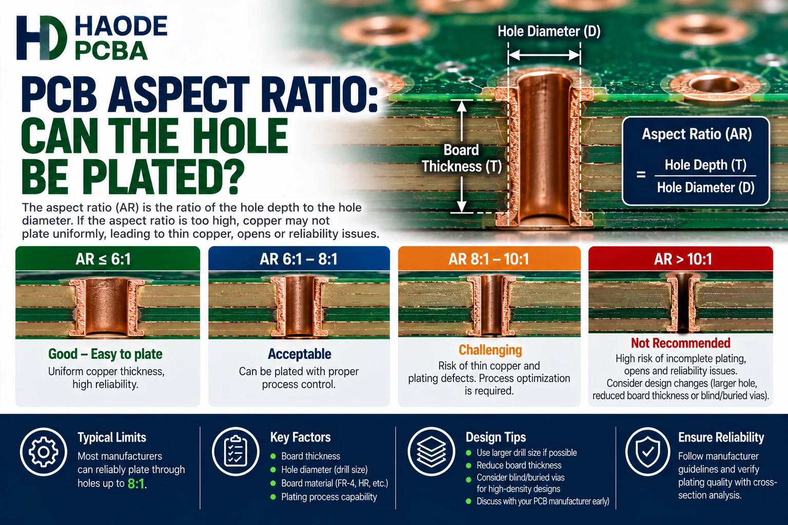
PCB aspect ratio equals the hole depth divided by the drilled-hole diameter. For a plated through hole, manufacturers normally compare finished board thickness with the mechanical drill diameter before plating. As the ratio increases, cleaning, chemical copper deposition, electrolytic plating, and inspection become more difficult.
For example, a 1.60 mm board with a 0.30 mm drilled hole has an aspect ratio of approximately 5.33:1:
1.60 mm ÷ 0.30 mm = 5.33
However, this number alone does not prove manufacturability. Material, hole type, plating thickness, panel design, drill quality, copper chemistry, and supplier process capability also control the result.
Therefore, buyers should ask more than, “Can you manufacture a 10:1 PCB?” The more useful question is:
Can the supplier consistently clean and plate this specific hole through this specific material and board thickness while meeting the required minimum hole copper?
What Is PCB Aspect Ratio?
PCB aspect ratio describes the relationship between hole depth and hole diameter.
The general formula is:
PCB Aspect Ratio = Hole Depth ÷ Drilled-Hole Diameter
For a through hole:
Through-Hole Aspect Ratio = Finished PCB Thickness ÷ Mechanical Drill Diameter
For a blind via:
Blind-Via Aspect Ratio = Via Depth ÷ Via Diameter
The calculation appears simple. Nevertheless, designers must define the numerator and denominator correctly.
Hole Depth
For an ordinary plated through hole, the hole passes through the full board thickness. Therefore, the finished board thickness normally represents the hole depth.
For a blind via, use the actual drilling or plating depth rather than total board thickness.
For a buried via, use the thickness of the laminated subassembly through which the hole passes.
Hole Diameter
For manufacturing analysis, many fabricators use the mechanical drill diameter or minimum drilled diameter before plating.
Do not automatically use the finished-hole diameter. Copper plating reduces the open diameter but does not increase the original space available for hole cleaning and metallization.
The distinction between tool size, drilled size, and finished opening is explained in our PCB drill size versus finished hole size article.
PCB Aspect Ratio Calculation Examples
The following examples show how board thickness and hole diameter change the ratio.
| Hole Type | Hole Depth | Drilled Diameter | Calculated Aspect Ratio |
|---|---|---|---|
| Through Hole | 1.60 mm | 0.40 mm | 4.00:1 |
| Through Hole | 1.60 mm | 0.30 mm | 5.33:1 |
| Through Hole | 2.00 mm | 0.25 mm | 8.00:1 |
| Through Hole | 3.20 mm | 0.30 mm | 10.67:1 |
| Blind Via | 0.20 mm | 0.15 mm | 1.33:1 |
| Blind Via | 0.15 mm | 0.10 mm | 1.50:1 |
These calculations describe geometry only. They do not automatically classify the holes as acceptable or unacceptable.
For example, two suppliers may both advertise 10:1 capability. However, one may support that ratio only with:
- A larger minimum drill
- Standard FR-4
- Limited panel dimensions
- Reduced production stack height
- A specific copper thickness
- Longer plating time
- Additional microsection inspection
- Prototype quantities
The second supplier may have a controlled production process for several materials and higher volumes.
Therefore, buyers should never compare aspect-ratio numbers without comparing the conditions behind them.
Should PCB Aspect Ratio Use Drill Size Or Finished Hole Size?
The quotation and engineering documents should state which diameter the calculation uses.
Consider an illustrative plated through hole:
| Dimension | Example Value |
|---|---|
| Finished Board Thickness | 1.60 mm |
| Mechanical Drill Diameter | 0.35 mm |
| Finished-Hole Target | 0.30 mm |
Using the drill diameter:
1.60 ÷ 0.35 = 4.57:1
Using the finished-hole target:
1.60 ÷ 0.30 = 5.33:1
The same hole produces two different reported ratios.
This difference can cause confusion between designers, purchasing teams, and PCB suppliers. Therefore, write the calculation basis in the RFQ instead of sending only the ratio.
An automotive addendum to IPC-6012 explicitly states that via holes should use a minimum drilled-size specification to secure sufficient aspect ratio. This supports the practice of defining the pre-plating hole dimension rather than relying only on the finished opening.
Why Finished Hole Still Matters
Although the drilled diameter controls the basic manufacturing ratio, the finished-hole dimension remains essential for:
- Component-lead fit
- Press-fit connectors
- Fasteners
- Pin insertion
- Solder fill
- Connector alignment
- Electrical and mechanical tolerances
Consequently, a complete drawing should specify both the finished-hole requirement and the manufacturing information needed to evaluate plating capability.
Why High PCB Aspect Ratio Makes Plating Difficult
A deep, narrow hole restricts chemical movement through the barrel. As a result, each wet process becomes harder to control.
Hole Cleaning
Drilling can leave resin smear and debris on the exposed internal copper. The manufacturer must remove this material before metallization.
However, chemistry must enter, circulate through, and exit the entire hole. A deeper and narrower hole makes that exchange more difficult.
If cleaning remains incomplete, later copper layers may deposit over contamination instead of bonding directly to the internal copper.
The PCB desmear process explains how manufacturers expose clean internal-layer copper before metallization.
Chemical Copper Deposition
After desmear, the manufacturer creates a thin conductive layer over the nonconductive hole wall. This initial layer must cover the full barrel, including the center of the hole.
High aspect ratio can reduce solution exchange and increase the risk of:
- Incomplete activation
- Thin electroless copper
- Skip plating
- Local discontinuity
- Poor connection to internal pads
Our PCB electroless copper article covers activation, deposition, coverage, and process-control requirements.
Electrolytic Copper Plating
Electrolytic plating builds the functional copper thickness in the barrel. Nevertheless, current density and solution movement do not remain identical at the hole entrance and center.
Copper often deposits more readily near the outer surfaces and hole mouths. In contrast, the center of a high-ratio hole may receive less copper.
Therefore, thicker surface copper does not automatically prove sufficient copper at the barrel center.
Solution Movement
The plating line must move fresh chemistry through the hole and remove depleted solution and reaction products.
Relevant controls include:
- Agitation
- Panel movement
- Solution flow
- Air or eductor design
- Current density
- Plating waveform
- Bath composition
- Additive balance
- Temperature
- Panel loading
- Hole density
A laboratory result from one coupon does not guarantee the same distribution across a large production panel.
PCB Aspect Ratio And Throwing Power
Throwing power describes a plating process’s ability to deposit copper inside the hole relative to more accessible areas.
A simplified evaluation may compare copper thickness at the barrel center with copper near the surface or hole entrance.
For example:
Microdistribution = Minimum Hole Copper ÷ Surface Copper × 100
The exact terminology and calculation method should follow the supplier’s controlled procedure.
A lower value indicates that the process deposits less copper in the difficult center region. Therefore, a high aspect ratio may require longer plating time or a more capable plating process to achieve the specified minimum.
However, simply extending plating time can create other problems:
- Excessive surface copper
- Reduced trace-and-space capability
- Increased etching difficulty
- Uneven copper distribution
- Higher cost
- Longer production cycle
The interaction between hole geometry, current distribution, and plating chemistry is explained in our PCB throwing power article.
IPC technical research on high-throw acid-copper processes evaluated boards from 1.6 mm to 3.2 mm thick with hole geometries ranging across aspect ratios from 4.6 to 16. The study also identified mass transfer and current density as important plating variables. Therefore, aspect ratio describes difficulty, but the plating process determines the achievable copper distribution.
What Defects Can High PCB Aspect Ratio Cause?
High aspect ratio does not create one single defect. Instead, it reduces the process window for several operations.
| Potential Defect | Possible Mechanism | Useful Inspection |
|---|---|---|
| Plating Void | Incomplete activation or copper coverage | Microsection and electrical test |
| Thin Center Copper | Poor current or solution distribution | Microsection thickness measurement |
| Inner-Layer Separation | Smear or weak metallurgical connection | Microsection after thermal stress |
| Barrel Crack | Insufficient copper or thermal fatigue | Thermal cycling and microsection |
| Skip Plating | Local failure of conductive seed layer | Microsection or resistance testing |
| Nodules Or Roughness | Unstable plating conditions | Visual and microsection inspection |
| Drill Smear | Inadequate cleaning of the hole wall | Microsection |
| Hole Too Small | Excess plating or inaccurate drill compensation | Pin gauge or dimensional measurement |
| Intermittent Connection | Marginal internal interface | Resistance monitoring and thermal testing |
A PCB plating void may remain small enough for a board to pass an initial continuity test. Nevertheless, thermal and mechanical stress can enlarge its effect during service.
Similarly, PCB barrel cracks may develop after repeated expansion and contraction even when the new bare board passes electrical testing.
Does Higher PCB Aspect Ratio Automatically Mean Lower Reliability?
Not automatically.
A properly manufactured high-aspect-ratio hole can perform reliably. However, the design places greater demands on drilling, cleaning, metallization, copper distribution, and verification.
Reliability also depends on:
- Hole copper thickness
- Copper ductility
- Laminate Z-axis expansion
- Glass transition temperature
- Hole-wall quality
- Internal pad connection
- Board thickness
- Thermal excursion
- Reflow cycles
- Operating-temperature range
- Vibration and mechanical loading
Therefore, two holes with the same ratio may not provide the same reliability.
For example, a thicker board can experience greater Z-axis expansion across the plated barrel during thermal cycling. Meanwhile, a smaller hole may contain thinner copper at its center. Together, these conditions can increase barrel fatigue.
IPC-published research found that a fixed-size plated through hole becomes less reliable as board thickness and aspect ratio increase. The research also emphasizes that board thickness and hole structure interact rather than acting as isolated variables.
Through-Hole, Blind-Via, And Microvia Aspect Ratio
Designers should not use one capability number for every hole type.
Plated Through Holes
A plated through hole crosses the entire finished board. Therefore, total board thickness affects the ratio.
Mechanical drilling, desmear, electroless copper, and electrolytic plating must all work through the full barrel.
Mechanically Drilled Blind Vias
A blind via connects an external layer to one or more internal layers without passing through the entire PCB.
Use the actual blind-hole depth in the numerator. However, controlled-depth drilling, bottom geometry, debris removal, and plating access also affect capability.
Buried Vias
A buried via exists inside a laminated subassembly. Its ratio depends on the subassembly thickness at the stage when the manufacturer drills and plates it.
Later lamination cycles add thermal and mechanical stress. Therefore, evaluate both manufacturing ratio and accumulated lamination exposure.
Laser-Drilled Microvias
Microvias require a different analysis because laser drilling creates a tapered hole with a capture land and target land.
Relevant dimensions include:
- Dielectric depth
- Top diameter
- Base diameter
- Target-land diameter
- Capture-pad diameter
- Target contact
- Copper fill
- Stack structure
Consequently, a single diameter may not fully describe microvia manufacturability.
For stacked or complex HDI constructions, the fabricator may divide the board into substructures and use PCB sequential lamination rather than drilling one narrow hole through the complete board.
What Is The Maximum Acceptable PCB Aspect Ratio?
There is no universal maximum that applies to every PCB manufacturer and design.
Commercial capability statements often list ratios such as 6:1, 8:1, 10:1, or higher. However, these values may represent different conditions.
Before accepting a capability number, ask:
- Does it use drill diameter or finished-hole diameter?
- Does it apply to prototypes or volume production?
- What minimum drill size supports the ratio?
- What maximum board thickness supports it?
- Which laminate materials qualify?
- What minimum hole copper must remain?
- Does it apply to through holes, blind vias, or both?
- What panel size did the supplier qualify?
- How many boards enter one drilling stack?
- Does the supplier require special plating?
- What inspection and sampling support the claim?
- Does the quoted price include those controls?
A supplier may manufacture one test coupon at a high ratio but lack a stable production window for a large multilayer panel. Therefore, capability should describe repeatable production, not only the best isolated result.
IPC-6012F defines qualification and performance requirements for rigid boards and includes requirements for microsection evaluation, hole copper plating, structural integrity, and thermal stress. Therefore, aspect ratio should connect to finished-product evidence rather than remain only a design calculation.
How To Reduce PCB Aspect Ratio
Designers have several options when a hole exceeds the supplier’s controlled capability.
Increase The Drill Diameter
A larger drill immediately reduces the ratio.
For a 2.00 mm board:
- 0.20 mm drill: 10.00:1
- 0.25 mm drill: 8.00:1
- 0.30 mm drill: 6.67:1
- 0.40 mm drill: 5.00:1
However, a larger hole also requires a larger pad and anti-pad. Therefore, check annular ring, routing channels, plane clearance, and impedance before making the change.
Reduce Finished Board Thickness
A thinner PCB lowers the ratio without changing the hole.
Nevertheless, board thickness also affects stiffness, connector fit, component leads, controlled impedance, and enclosure dimensions. Our PCB thickness article explains these tradeoffs.
Use Blind Or Buried Vias
Blind and buried vias shorten the hole depth. However, they add process steps, sequential lamination, inspection requirements, and cost.
Use them when density or electrical performance justifies the manufacturing complexity.
Change The Layer Stackup
The designer may move connected layers closer together or reorganize the stackup so that a blind via spans fewer dielectric layers.
However, every stackup change can affect:
- Controlled impedance
- Reference-plane continuity
- Signal return paths
- Dielectric spacing
- Copper balance
- Lamination symmetry
Therefore, the PCB designer and fabricator should approve the revised stackup together.
Review Whether Every Small Hole Is Necessary
Some designs use one default via size across the entire PCB. However, power vias, thermal vias, test vias, and signal vias do not always need identical dimensions.
Using larger holes where routing density permits can reduce plating risk without changing the densest regions.
How To Inspect High PCB Aspect Ratio Holes
Inspection should examine the most difficult part of the barrel, not only the surface opening.
Microsection Measurement
A PCB microsection can reveal:
- Copper thickness near the top
- Copper thickness at the barrel center
- Copper thickness near the bottom
- Plating voids
- Resin smear
- Etchback condition
- Inner-layer contact
- Barrel roughness
- Cracks after thermal stress
The report should identify the minimum measured copper rather than only the average.
IPC’s public test-method library lists methods for microsectioning and plated-through-hole structure evaluation. These methods support repeatable specimen preparation and structural inspection.
Panel Location
Plating performance can vary across the panel. Therefore, samples should represent relevant locations, such as:
- Panel center
- Panel edge
- High-hole-density area
- Low-hole-density area
- Smallest drill group
- Critical connector region
A coupon located in an easy plating region may not represent the worst functional holes.
Thermal Stress
A hole may look acceptable before thermal exposure but reveal cracks or interface separation afterward.
For higher-reliability products, the inspection plan may include:
- Solder-float testing
- Reflow simulation
- Thermal shock
- Thermal cycling
- Interconnect stress testing
- Resistance monitoring
Select the method according to product use, applicable specifications, and customer requirements.
What Buyers Should Put In The RFQ
Do not submit only “maximum aspect ratio 10:1.”
Instead, provide:
- Nominal finished board thickness
- Board-thickness tolerance
- Smallest mechanical drill
- Finished-hole requirements
- Plated and non-plated hole identification
- Hole type
- Layer count
- Approved stackup
- Material family
- Copper weight
- Required hole copper
- Annular-ring requirement
- Panel dimensions
- Critical hole locations
- Controlled-impedance requirements
- Applicable IPC document and revision
- Product performance class
- Thermal-test requirement
- Microsection sample quantity
- Prototype and production volumes
Additionally, ask the supplier to state:
- Aspect-ratio calculation basis
- Maximum qualified ratio
- Standard production ratio
- Special-process threshold
- Minimum drill at the quoted thickness
- Expected finished-hole tolerance
- Hole copper measurement method
- Coupon design
- Sampling plan
- Any design changes required
This information makes different quotations comparable.
PCB Aspect Ratio DFM Checklist
Before releasing the fabrication data, confirm:
- Did you calculate every hole type?
- Did you use the drilled diameter rather than automatically using the finished opening?
- Did you use maximum finished board thickness for worst-case screening?
- Did you use actual depth for blind and buried vias?
- Does the drill table distinguish plated and non-plated holes?
- Can the selected drill produce the required finished hole?
- Does the pad maintain enough annular ring?
- Does the anti-pad maintain enough clearance?
- Can chemistry circulate through the hole?
- Can the supplier achieve minimum center-barrel copper?
- Does the material require special desmear control?
- Does the panel contain dense and sparse hole regions?
- Has the supplier qualified the ratio at the actual panel size?
- Does the inspection plan sample relevant panel locations?
- Will the board experience several lead-free reflow cycles?
- Does the product require thermal cycling or stress testing?
- Would a larger drill reduce risk?
- Would a thinner stackup solve the problem?
- Would blind vias or sequential lamination provide better margin?
- Has the manufacturer completed a PCB DFM review?
Frequently Asked Questions About PCB Aspect Ratio
What Is A Good PCB Aspect Ratio?
A lower ratio generally provides a wider manufacturing process window. However, a “good” value depends on board construction, drill diameter, material, required hole copper, supplier capability, and reliability target.
Therefore, use the fabricator’s qualified production capability rather than a universal internet value.
Is PCB Aspect Ratio Based On Finished Hole Size?
Manufacturers commonly use drilled-hole diameter for plating-process analysis. However, some documents and capability tables may use finished-hole diameter.
Always state the calculation basis so that the designer and supplier evaluate the same geometry.
Does A Smaller Via Always Increase PCB Cost?
Not always. Nevertheless, a smaller drill can increase tool wear, drilling time, aspect ratio, plating difficulty, inspection requirements, and rejection risk.
The cost increase depends on whether the hole remains inside the supplier’s standard process window.
Can A High Aspect Ratio Hole Pass Electrical Test?
Yes. Electrical testing may confirm continuity even when the barrel contains thin copper or limited reliability margin.
Therefore, high-ratio holes may also need microsection and thermal evidence.
Can More Plating Solve A High Aspect Ratio Problem?
Additional plating time may increase hole copper. However, it can also create excessive surface copper and make fine-line etching more difficult.
The supplier must improve copper distribution, not merely deposit more copper everywhere.
Does Aspect Ratio Affect Annular Ring?
Aspect ratio and annular ring describe different dimensions.
Aspect ratio compares hole depth with hole diameter. Annular ring measures the copper remaining between the hole and pad edges.
However, a very small drill often accompanies a small pad. Therefore, dense designs may face both plating and registration risk at the same time.
Do Non-Plated Holes Have A Plating Aspect Ratio?
Non-plated holes do not require hole-wall copper. Therefore, the plating aspect ratio does not apply in the same way.
Even so, deep, small non-plated holes can still create drilling, debris-removal, positional, and dimensional challenges.
Is A Blind Via Always Easier To Plate?
Not necessarily. A blind via has a shorter depth, but chemistry can enter and exit from only one side. Bottom shape, trapped gas, debris, and target-pad geometry also affect processing.
Therefore, evaluate blind vias according to their specific drilling and plating method.
Final Recommendations For PCB Aspect Ratio
PCB aspect ratio provides a fast way to screen hole manufacturability, but it does not replace process capability or finished-board inspection.
For reliable plated holes:
- Calculate depth divided by drilled-hole diameter.
- State whether the denominator uses drill or finished size.
- Use worst-case board thickness during DFM.
- Separate through-hole, blind-via, buried-via, and microvia calculations.
- Review desmear and metallization access.
- Confirm center-barrel copper capability.
- Evaluate throwing power rather than surface copper alone.
- Request representative microsections.
- Include thermal testing when product risk requires it.
- Reduce the ratio before adding unnecessary process complexity.
- Define the calculation and inspection requirements in the RFQ.
The most important relationship is:
Board Thickness And Hole Diameter → PCB Aspect Ratio → Cleaning And Plating Difficulty → Minimum Hole Copper → Thermal Reliability
When the design approaches a supplier’s capability limit, do not approve it from a capability table alone. Ask for the qualified material, drill basis, minimum hole copper, panel conditions, sampling plan, and supporting microsection data.