
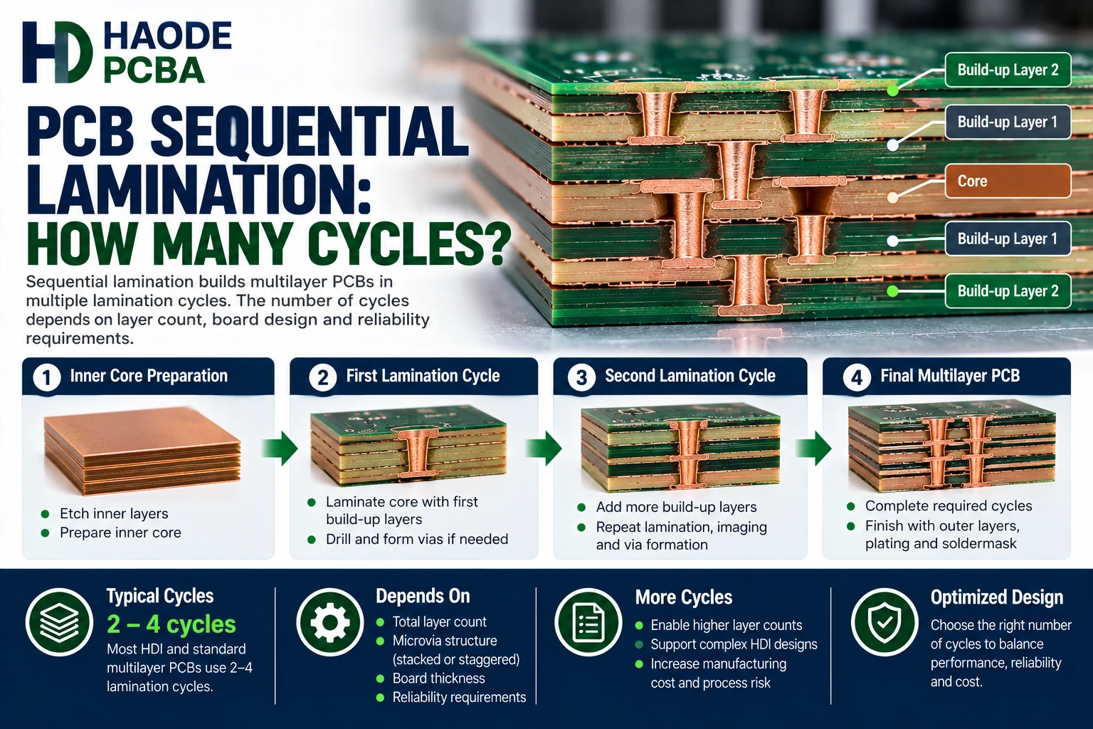
PCB sequential lamination builds a complex PCB through two or more lamination cycles. Manufacturers use it when they must drill, plate, fill, or image an internal structure before adding another dielectric and copper layer above it.
A conventional multilayer PCB may require only one main lamination cycle. In contrast, a 1+N+1 HDI structure commonly requires a laminated core plus one build-up cycle, while a 2+N+2 structure commonly adds another build-up cycle.
However, buyers should not estimate cost from the layer count alone. The actual number of cycles depends on the buried vias, microvia layer pairs, stacking method, copper filling, and the manufacturer’s production flow.
The most important relationship is:
Structures That Must Be Completed Before Burial → Additional Lamination Stages → More Processing, Registration, Testing, And Yield Risk
What Is PCB Sequential Lamination?
PCB sequential lamination means that an already laminated PCB subassembly undergoes one or more additional lamination cycles.
During each cycle, the manufacturer adds dielectric material, copper foil, another prepared subassembly, or a combination of these materials. Heat and pressure then bond the new structure to the existing subassembly.
Isola defines sequential lamination as a group of technologies in which manufacturers laminate previously laminated subparts to additional copper layers or other subparts. It also notes that a sequentially laminated PCB experiences at least two lamination cycles.
A typical PCB sequential lamination flow may include:
- Image and etch the inner layers.
- Laminate the core subassembly.
- Drill and plate buried vias.
- Add another dielectric and copper layer.
- Laminate again.
- Form blind microvias.
- Plate or copper-fill the microvias.
- Repeat the build-up process when additional HDI layers are required.
- Complete the outer-layer pattern, solder mask, finish, and routing.
The exact sequence changes with the stackup. Therefore, the buyer should request a process-flow explanation rather than assuming that every layer requires a separate press cycle.
Why Does A PCB Need Sequential Lamination?
A PCB needs sequential lamination when the fabricator cannot create all required interconnections after one final pressing operation.
Buried Vias
A buried via connects internal layers without reaching either finished outer surface.
The manufacturer must normally:
- Laminate the relevant internal layers
- Drill the subassembly
- Plate the buried holes
- Inspect the structure
- Laminate additional layers around it
Once the fabricator buries the via, conventional drilling can no longer reach it. Therefore, the buried-via subassembly creates an additional lamination stage.
Multiple Microvia Levels
A laser microvia typically connects adjacent build-up layers. If the design requires several microvia levels, the manufacturer adds them sequentially.
For a two-level structure, the factory may:
- Laminate the first build-up dielectric.
- Laser-drill and plate the first microvia level.
- Add another dielectric and copper layer.
- Laminate again.
- Drill and plate the second microvia level.
Stacked Microvias
An upper stacked microvia uses the filled lower microvia as its target. Consequently, the lower structure must be completed, copper-filled, and prepared before the next lamination cycle.
Our stacked vs staggered microvias article explains the reliability and routing differences between the two arrangements.
Mixed Blind And Buried Structures
A PCB may combine:
- Mechanically drilled buried vias
- Laser microvias
- Through holes
- Blind mechanical vias
- Stacked microvias
- Staggered microvias
- Via-in-pad structures
Different drilling depths and start-stop layers can force the manufacturer to divide these structures across several subassemblies and lamination stages.
How Do You Count PCB Sequential Lamination Cycles?
Start by identifying which vias or circuits must be manufactured before another layer covers them.
A new cycle normally occurs when the manufacturer must:
- Complete a structure on the current surface.
- Add dielectric and copper above that structure.
- Press the assembly again.
- Create another structure from the new surface.
Typical Cycle Estimates
| PCB Construction | Typical Total Lamination Cycles | Why |
|---|---|---|
| Conventional Multilayer Without Buried Vias | 1 | Inner layers enter one main multilayer pressing operation |
| Buried-Via Core With Outer Layers | At Least 2 | The core requires drilling and plating before final lamination |
| 1+N+1 HDI | Commonly 2 | One core lamination plus one build-up cycle |
| 2+N+2 HDI | Commonly 3 | Core plus two build-up stages |
| 3+N+3 HDI | Commonly 4 | Core plus three build-up stages |
| Asymmetric 2+N+1 HDI | Process Dependent | Unequal build-up may require special balancing or flow |
| Coreless HDI | Process Dependent | Layer-pair construction changes the conventional core sequence |
| Mixed Buried Via And Stacked Microvia | Often More Than The Notation Suggests | The buried-via subassembly may add an earlier cycle |
These estimates describe common process flows, not guaranteed quotations.
Two suppliers may report different cycle counts because one counts the original core lamination while another reports only the additional sequential build-up cycles.
Therefore, ask the supplier to state both:
- Total press cycles experienced by the finished PCB
- Additional build-up cycles after the core or subassembly
This distinction prevents a “two-cycle” quotation from being compared incorrectly with another supplier’s “three-cycle” quotation.
Does Each HDI Layer Require One Lamination Cycle?
Not necessarily.
Manufacturers can often add one build-up layer to both sides of a symmetrical core during the same pressing operation. Therefore, a 1+N+1 construction commonly needs one build-up cycle rather than two separate cycles.
Likewise, a 2+N+2 construction can add the first build-up layers to both sides simultaneously, followed by the second build-up layers in another cycle.
However, several factors can change the flow:
- Asymmetrical build-up
- Different materials on opposite sides
- Buried vias inside the core
- Different microvia depths
- Unusual copper weights
- Mixed rigid and flex regions
- Local cavities
- Embedded components
- Manufacturer equipment limitations
Consequently, the notation describes the final structure more clearly than it describes the exact factory process.
What Do 1+N+1 And 2+N+2 Mean?
The notation describes the number of build-up layers on each side of a central core or multilayer subassembly.
1+N+1 HDI
A 1+N+1 board contains:
- One build-up layer on the top
- An N-layer central core
- One build-up layer on the bottom
For example, a 1+4+1 construction has six finished copper layers.
2+N+2 HDI
A 2+N+2 board contains:
- Two build-up layers on the top
- An N-layer central core
- Two build-up layers on the bottom
For example, a 2+6+2 construction has ten finished copper layers.
Asymmetric HDI
A 2+N+1 construction has two build-up layers on one side and one on the other.
Although it contains fewer total layers than a 2+N+2 structure, it may create more difficult mechanical balancing and process-planning problems.
IPC-2226A uses notation such as 2[C]1 to identify the number of HDI layers on each side of a core. It also classifies several HDI architecture types based on the core and build-up arrangement.
However, IPC’s current revision table lists IPC-2226A as no longer maintained. Therefore, buyers can use its terminology to communicate structure, but they should confirm which current design and performance documents govern the purchase.
Do Stacked Microvias Require More Cycles Than Staggered Microvias?
Not when both structures connect the same layer pairs.
For example, stacked and staggered microvias in a 2+N+2 PCB normally require the same number of build-up lamination stages.
The difference lies in the processing between those stages.
Stacked Structure
Before adding the next layer, the manufacturer normally needs to:
- Copper-fill the lower microvia
- Control the fill dimple
- Create sufficient cap copper
- Prepare a flat target for the next microvia
- Maintain tight registration between levels
Staggered Structure
The upper microvia lands on a separate pad. Therefore, the lower microvia may not need to support another via directly above it.
However, the manufacturer must still add each build-up dielectric sequentially.
Thus:
Stacked Versus Staggered Changes Process Complexity And Risk, But It Does Not Automatically Change The Number Of Build-Up Layers.
The microvia copper filling process becomes especially important when a filled lower via supports the next stacked level.
Can A Skipped Microvia Reduce Lamination Cycles?
Potentially, but it creates different manufacturing challenges.
A skipped microvia passes through more than one dielectric layer and terminates on a deeper target pad. In some designs, it can reduce the need to build and drill each adjacent layer separately.
However, deeper laser drilling can create:
- A higher depth-to-diameter ratio
- More difficult debris removal
- Greater target-pad exposure risk
- More difficult metallization
- Reduced plating uniformity
- Tighter laser-depth control
- A narrower process window
Therefore, a skipped microvia should not serve only as a cost-reduction shortcut.
The manufacturer must compare:
- Lamination cycles saved
- Laser-drilling capability
- Via geometry
- Plating capability
- Target-pad size
- Reliability testing
- Production yield
A lower theoretical cycle count does not guarantee a lower total cost.
How Does PCB Sequential Lamination Affect Cost?
Each additional cycle adds more than press time.
It can add:
- Material preparation
- Layup
- Registration
- Lamination
- Imaging
- Etching
- Laser or mechanical drilling
- Desmear
- Metallization
- Copper plating
- Copper filling
- Planarization
- Inspection
- Handling
- Engineering control
Yield Compounds Across Stages
Suppose each major build stage has a high individual yield. The final yield still decreases as the number of dependent stages increases.
A defect introduced during an early stage may not become visible until the manufacturer has completed several expensive later operations.
Therefore, the cost increase includes:
- More direct processing
- More inspection
- Longer lead time
- Higher scrap value
- Lower cumulative yield
- More qualification work
Layer Count Alone Does Not Predict Price
A ten-layer conventional multilayer PCB may cost less than an eight-layer HDI PCB that requires buried vias, two sequential build-up stages, copper filling, and reliability coupons.
Buyers should compare quotations using:
- Total lamination cycles
- Microvia layer pairs
- Buried-via structures
- Copper-fill requirements
- Line and space
- Material
- Test requirements
- Order quantity
How Does Sequential Lamination Affect Lead Time?
Sequential lamination creates dependent operations. The factory cannot start the next build-up stage until it completes and verifies the previous one.
A simplified flow may be:
Core Fabrication → First Lamination → Drilling And Plating → Second Lamination → Microvia Formation → Third Lamination → Final Fabrication
The manufacturer may also need intermediate inspections before burying a structure.
Lead-time drivers include:
- Material availability
- Press scheduling
- Laser-drilling capacity
- Copper-fill capacity
- Registration verification
- Microsection approval
- Failed-stage rework limitations
- Test-coupon processing
Because later layers depend on earlier results, the factory cannot parallelize every operation.
For prototypes, engineering review and coupon preparation can take a significant share of the schedule. For volume production, stable repeat orders may shorten planning time, but the physical process sequence remains.
How Does PCB Sequential Lamination Affect Reliability?
PCB sequential lamination does not automatically make a board unreliable. However, every additional cycle adds thermal and mechanical history.
Repeated Heat Exposure
Previously cured subassemblies experience additional heating during later lamination cycles.
The material system must tolerate:
- Repeated cure temperatures
- Pressure
- Cooling
- Moisture exposure between stages
- Chemical processing
- Assembly reflow after fabrication
CTE Mismatch
Copper, resin, and glass reinforcement expand at different rates.
Isola’s sequential-lamination application note identifies copper-to-resin expansion mismatch as a major stress factor. It also discusses resin cracks, delamination, resin voids, and failed microvia connections as possible concerns in thicker, higher-layer-count structures.
Buried Pad Stress
When a pad sits below additional glass-reinforced dielectric, thermal expansion can place tensile and shear stress around the copper-resin interface.
The risk depends on:
- Resin thickness above the pad
- Glass position
- Pad diameter
- Via type
- Copper thickness
- Material properties
- Board thickness
- Number of thermal cycles
Microvia Interface Risk
Additional build-up levels create more microvia interfaces. Stacking places those interfaces in a vertical load path.
The PCB microvia reliability assessment should therefore consider both the final geometry and the complete lamination history.
Does High Tg Guarantee Sequential Lamination Reliability?
No. Tg describes the temperature range in which the resin changes from a relatively rigid condition to a more compliant condition. It does not describe every property that affects repeated lamination.
Material review may also include:
- Decomposition temperature
- Z-axis CTE
- Time to delamination
- Resin content
- Resin flow
- Cure behavior
- Moisture absorption
- Copper adhesion
- Glass style
- Laser-drilling response
- Desmear compatibility
A high-Tg material can still create problems if its resin flow does not suit the copper pattern or if the desmear process cannot prepare the laser-drilled surface consistently.
Therefore, buyers should allow the PCB manufacturer to recommend a qualified material construction while controlling essential electrical, thermal, and regulatory requirements.
Why Does Resin Flow Matter?
During lamination, softened resin must fill spaces around copper features without leaving voids or causing excessive thickness variation.
Insufficient resin flow can create:
- Resin starvation
- Lamination voids
- Poor bonding
- Exposed glass
- Local dielectric weakness
Excessive resin flow can create:
- Dielectric thickness variation
- Registration movement
- Resin squeeze-out
- Reduced local resin content
- Impedance variation
Copper-filled microvias, large pads, heavy copper, and uneven copper distribution change the surface topography that the prepreg must cover.
Therefore, the manufacturer should select prepreg style and resin content from the actual copper pattern, not only the nominal finished thickness.
Why Are Asymmetric Build-Ups More Difficult?
A symmetric 2+N+2 construction adds similar materials and copper structures to both sides during each build-up stage.
An asymmetric construction may create differences in:
- Copper coverage
- Dielectric thickness
- Resin flow
- Thermal expansion
- Cooling stress
- Press pressure distribution
As a result, the PCB may develop bow, twist, or registration movement.
The factory may recommend:
- Adding a balancing layer
- Adjusting copper distribution
- Changing prepreg construction
- Modifying the build sequence
- Using temporary support
- Converting the stackup to a symmetric structure
Our PCB warpage article explains why total board thickness alone does not control flatness.
How Does Sequential Lamination Affect Impedance?
Sequential lamination influences the dielectric spacing between signal traces and reference planes.
The final spacing depends on:
- Prepreg resin content
- Copper thickness
- Copper density
- Glass style
- Press parameters
- Filled-via topography
- Core thickness
- Etched copper geometry
Therefore, the designer should not assign final impedance dimensions using only generic material data.
Instead, the PCB manufacturer should provide:
- Production dielectric targets
- Copper thickness by layer
- Expected pressed thickness
- Trace-width adjustment
- Impedance coupon design
- Finished tolerance
A stackup change that reduces one lamination cycle can also change reference-plane locations and dielectric thickness. Consequently, the electrical design requires another review.
How Should Sequentially Laminated PCBs Be Inspected?
Inspection should verify both hidden structures and finished-board performance.
Intermediate Inspection
Before burying a via or circuit, the manufacturer may inspect:
- Drilling quality
- Hole cleanliness
- Plating coverage
- Copper thickness
- Via filling
- Registration
- Surface condition
Once another layer covers the structure, direct inspection becomes more difficult.
Final Microsection
A PCB microsection can evaluate:
- Buried-via plating
- Microvia interfaces
- Copper fill
- Dielectric thickness
- Registration
- Resin voids
- Delamination
- Internal copper condition
However, the section must intersect the relevant feature correctly.
Thermal Performance Testing
A structurally acceptable cross-section does not prove that every microvia remains stable during heating.
For complex HDI builds, microvia reflow testing can monitor resistance throughout representative assembly cycles.
Longer-term PCB IST testing can then evaluate progressive interconnect degradation.
Which Standards Apply To PCB Sequential Lamination?
No single note such as “IPC compliant” completely defines a sequentially laminated PCB.
The purchasing documents may need to reference:
- A generic printed-board design standard
- A rigid-board or rigid-flex design standard
- Applicable material specifications
- Rigid-board performance requirements
- Printed-board acceptability criteria
- Applicable test methods
- Customer-specific reliability requirements
IPC-6012F covers qualification and performance requirements for rigid printed boards, including constructions with blind vias, buried vias, and microvias.
However, the drawing must still define:
- Performance class
- Standard revision
- HDI structure
- Materials
- Stackup
- Via requirements
- Inspection
- Thermal testing
- Acceptance criteria
The standard does not select the correct lamination architecture for the buyer.
What Should Buyers Include In The RFQ?
A useful PCB sequential lamination RFQ should provide:
- Finished layer count
- Proposed stackup
- HDI notation
- Via start and stop layers
- Buried-via structure
- Stacked and staggered microvias
- Microvia diameter and target size
- Copper-fill requirements
- Finished board thickness
- Copper weight by layer
- Controlled-impedance targets
- Material requirements
- Surface finish
- Applicable IPC class and revision
- Reflow profile
- Reliability-test requirements
- Prototype and production quantities
- Annual demand
- Required reports
Also ask the manufacturer to state:
- Total lamination cycles
- Additional sequential cycles
- Proposed process sequence
- Maximum qualified stacked levels
- Material substitutions
- Coupon plan
- Expected lead time
- Major cost drivers
A complete PCB assembly quote should separate genuine technical requirements from optional structures that only increase cost.
PCB Sequential Lamination DFM Checklist
Before releasing the design, verify:
- Does every buried via serve a necessary routing function?
- Can a through hole replace any buried structure?
- Can the design reduce one build-up level?
- Are stacked microvias genuinely required?
- Can staggered microvias fit?
- Could a skipped microvia reduce cycles without creating excessive plating risk?
- Is the build-up mechanically balanced?
- Has the manufacturer approved the material?
- Are microvia diameters compatible with dielectric depth?
- Is copper filling defined?
- Are cap copper and dimple limits functional?
- Does the stackup show every via layer pair?
- Are impedance values based on production dielectric thickness?
- Does the coupon reproduce every critical via structure?
- Does the thermal test reflect the assembly process?
- Have both total and additional lamination cycles been confirmed?
Complete this review through a formal PCB DFM checklist before freezing the layout.
Frequently Asked Questions About PCB Sequential Lamination
How Many Lamination Cycles Does A 1+N+1 PCB Need?
It commonly needs one core or subassembly lamination plus one build-up lamination cycle. However, buried vias or a special core structure may add processing stages.
How Many Cycles Does A 2+N+2 HDI PCB Need?
It commonly needs three total cycles: the central structure plus two build-up stages. The exact count depends on the buried-via and core process.
Does A 12-Layer PCB Require More Cycles Than An 8-Layer PCB?
Not necessarily. A conventional 12-layer PCB may use one primary lamination, while an eight-layer HDI board may require several sequential cycles.
Do Stacked Vias Increase The Lamination Count?
Not automatically. Stacked and staggered microvias connecting the same layer pairs usually require the same build-up stages. Stacking adds copper-fill, planarization, registration, and reliability demands.
Can Both PCB Sides Be Laminated At The Same Time?
Yes. Symmetrical build-up layers on both sides commonly enter the same pressing cycle.
Is Sequential Lamination Only Used For HDI PCBs?
No. Manufacturers also use it for buried-via multilayers, blind-via structures, embedded components, cavities, and some rigid-flex constructions.
Does More Lamination Always Mean Lower Reliability?
No. A qualified process can produce reliable sequentially laminated PCBs. However, additional cycles increase processing complexity and thermal history, so the design needs stronger control and evidence.
Can The Buyer Determine The Exact Cycle Count From Gerber Files?
Not reliably. The manufacturer also needs the stackup, via start-stop table, fill requirements, material, and intended fabrication sequence.
Why Do Two Suppliers Quote Different Lamination Counts?
They may count the original core lamination differently, or they may propose different subassembly and build-up processes. Ask both suppliers for a stage-by-stage process flow.
What Is The Best Way To Reduce Sequential Lamination Cost?
Reduce unnecessary HDI levels, buried-via structures, and stacked transitions before layout completion. A single removed build-up stage can eliminate several dependent fabrication operations.
Final Recommendations
PCB sequential lamination should be evaluated as a manufacturing sequence, not merely a finished layer stack.
For a reliable and commercially realistic design:
- Identify every structure that must be completed before burial.
- Separate total press cycles from additional build-up cycles.
- Do not assume every HDI layer needs a separate cycle.
- Remember that stacked and staggered vias may use the same number of build-up stages.
- Review asymmetric structures for warpage and registration risk.
- Select material from repeated-lamination requirements, not Tg alone.
- Use production dielectric values for impedance calculations.
- Include representative coupons and thermal testing.
- Ask suppliers to explain their proposed process flow.
- Remove unnecessary sequential stages before final layout release.
The number of lamination cycles affects cost, lead time, yield, material selection, registration, microvia reliability, and supplier availability. Confirming that number early prevents expensive stackup changes after the design has already entered production.