
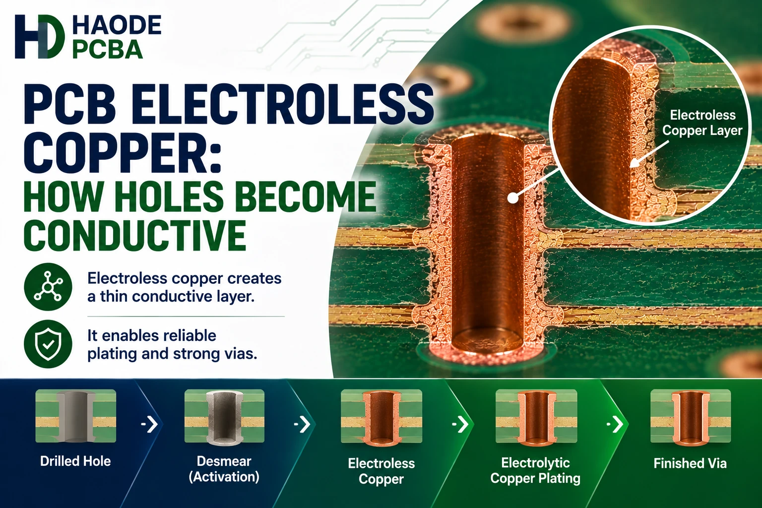
PCB electroless copper creates the first continuous conductive layer on drilled hole walls before electrolytic copper plating. The process succeeds only when copper covers the dielectric, bonds to exposed inner-layer copper, and remains intact during subsequent plating and thermal stress.
A finished hole may contain enough total copper yet still have a weak initial interface. Therefore, finished copper thickness alone cannot prove that electroless copper deposition was reliable.
Buyers should evaluate coverage, adhesion, interface location, process control, and post-thermal performance together.
What Is PCB Electroless Copper?
PCB electroless copper uses a chemical reduction reaction to deposit copper without applying external electrical current to the board.
This matters because a newly drilled hole exposes nonconductive resin and glass. Conventional electroplating cannot deposit copper uniformly on that surface until the manufacturer makes the hole wall conductive.
The process generally:
- Cleans and conditions the hole wall.
- Prepares exposed inner-layer copper.
- Applies a catalytic activation layer.
- Deposits an initial copper layer chemically.
- Creates a conductive path for electrolytic plating.
Before this stage, the PCB desmear process must remove resin smear and drilling contamination. Electroless copper cannot form a reliable interconnection if residue still covers the inner-layer copper.
MacDermid Alpha describes electroless copper plating as a primary metallization process that conditions the surface, applies catalytic activation, and deposits copper on nonconductive PCB structures before electroplating.
PCB Electroless Copper vs. Electrolytic Copper
Electroless and electrolytic copper perform different jobs in PCB manufacturing.
| Comparison | Electroless Copper | Electrolytic Copper |
|---|---|---|
| External Current Required | No | Yes |
| Can Start On Nonconductive Dielectric | Yes, After Activation | No |
| Primary Function | Create Initial Conductive Coverage | Build Most Of The Finished Copper Thickness |
| Main Control Challenge | Activation, Coverage, Adhesion, Bath Stability | Current Distribution, Throwing Power, Thickness Uniformity |
| Common Defects | Skips, Thin Coverage, Weak Interfaces, Bath Decomposition | Thin Centers, Excess Surface Copper, Nodules, Burning |
| Typical Verification | Backlight, Microsection, Process Coupons | Thickness Measurement, Microsection, Plating Distribution |
The electroless layer enables electroplating. In contrast, the electrolytic process builds the copper thickness needed for electrical, mechanical, and thermal performance.
Consequently, a manufacturer can produce continuous electroless copper but still develop poor PCB plating uniformity during electroplating.
The reverse can also occur: the finished barrel may appear thick, while a contaminated or weak interface remains beneath it.
How Does the PCB Electroless Copper Process Work?
A typical process contains several chemical stages. However, the exact sequence depends on the chemistry supplier, laminate, equipment, and metallization method.
Hole-Wall Conditioning
Conditioning changes the surface so that the catalyst can reach and attach to resin, glass, and other dielectric areas.
This stage becomes more difficult when the hole contains:
- Exposed glass bundles
- Filled resin
- Low-loss laminate
- Polyimide
- Rough drilling damage
- High aspect ratio
- Mixed dielectric materials
A conditioner that works well on conventional FR-4 may not provide equal coverage on every high-frequency or filled material.
Copper Microetch And Surface Preparation
The line must also prepare exposed copper surfaces without removing excessive copper.
Insufficient treatment may leave oxide or contamination. However, excessive microetch can change inner-layer geometry or reduce the remaining copper interface.
Therefore, the supplier should control copper removal as a process parameter rather than increasing it whenever an interconnect problem appears.
Catalytic Activation
Because resin and glass do not conduct electricity, the manufacturer applies a catalyst that initiates copper deposition on those surfaces.
Activation depends on:
- Surface cleanliness
- Conditioner compatibility
- Catalyst concentration
- Solution contamination
- Bath temperature
- Treatment time
- Panel loading
- Hole dimensions
- Rinsing between stages
Incomplete activation can create unplated areas even when the electroless copper bath itself remains within its chemical limits.
Electroless Copper Deposition
The activated panel enters the copper bath. The chemical reaction then deposits copper on the hole wall, exposed inner-layer copper, and other prepared surfaces.
The manufacturer must control:
- Copper concentration
- Reducing-agent concentration
- Complexing agents
- pH
- Temperature
- Bath loading
- Filtration
- Solution movement
- Deposition rate
- Bath age
- By-product accumulation
Moreover, uncontrolled particles or spontaneous bath decomposition can create roughness, nodules, or unstable deposits.
Post-Deposition Handling
After deposition, the manufacturer rinses and transfers the panel to the next process.
Long delays, contaminated rinses, poor drying, oxidation, or unsuitable pre-electroplate cleaning can weaken the connection between electroless and electrolytic copper.
Thus, the transfer condition matters as much as the deposition bath.
Why Are Small and Deep Holes More Difficult?
A high-aspect-ratio hole restricts chemistry exchange and makes trapped air more difficult to remove.
As the hole becomes deeper or smaller, the process may face:
- Incomplete wetting
- Trapped air bubbles
- Weak conditioner exchange
- Nonuniform catalyst coverage
- Reduced solution movement
- Difficult rinsing
- Residue entrapment
- Greater panel-position variation
Therefore, the manufacturer should compare hole diameter, board thickness, and PCB aspect ratio before selecting the metallization process.
If defects appear mainly in the smallest holes, the investigation should compare them with larger holes on the same panel. This comparison can help separate a general bath problem from a geometry-related exchange problem.
However, high aspect ratio does not prove that electroless copper caused the defect. Drilling, desmear, rinsing, and electrolytic plating may produce similar patterns.
How Much PCB Electroless Copper Is Enough?
There is no universal electroless copper thickness that guarantees a reliable PCB.
Some production lines use low-build chemistry, while others use higher-build processes. The appropriate target depends on:
- Metallization chemistry
- Horizontal or vertical equipment
- Hole geometry
- Laminate material
- Subsequent electroplating process
- Pattern-plating sequence
- Handling requirements
- Reliability qualification
The initial layer must provide continuous conductivity and survive transfer into subsequent processing. Nevertheless, depositing more chemical copper does not automatically improve reliability.
Excessive or poorly controlled deposition may increase:
- Deposit stress
- Surface roughness
- Nodules
- Bath instability
- Chemical consumption
- Processing time
- Fine-feature dimensional changes
More importantly, the finished plated-through-hole requirement generally concerns the completed hole-wall copper after all plating stages. It does not necessarily define the electroless portion separately.
Therefore, buyers should not compare suppliers only by asking, “How many microns of chemical copper do you deposit?” A better review asks whether the initial layer provides complete coverage and reliable interfaces for the specific board construction.
What Causes PCB Electroless Copper Voids?
A void forms when copper fails to cover part of the required hole wall or interface.
Possible causes include:
- Residual drill smear
- Loose drilling debris
- Incomplete conditioning
- Poor catalyst adsorption
- Air entrapment
- Inadequate solution exchange
- Contaminated chemistry
- Incorrect bath concentration
- Unstable pH or temperature
- Excessive panel loading
- Poor rinsing
- Material incompatibility
- Bath decomposition particles
The defect location provides useful evidence.
| Defect Pattern | Possible Process Area | Evidence To Check |
|---|---|---|
| Copper Missing From Resin Areas | Conditioning Or Activation | Backlight, conditioner records, catalyst control |
| Copper Missing Near Glass Bundles | Glass Coverage Or Material Compatibility | Microsection, material comparison |
| Isolated Voids Through The Hole | Air, Debris, Or Local Contamination | Multiple sections, wetting and agitation data |
| Voids Concentrated At Hole Centers | Solution Exchange Or Aspect Ratio | Hole-size comparison, panel loading |
| Defects At Inner-Layer Copper | Smear, Oxide, Residue, Or Weak Adhesion | Unetched section, interface analysis |
| Defects After Electroplating | Electroless Coverage Or Later Plating | Pre- and post-electroplate samples |
Not every PCB plating void begins in the electroless copper bath. Consequently, corrective action should follow defect localization rather than assumption.
Which Copper Interface Has Failed?
A plated hole contains several interfaces. Identifying the failed interface helps separate desmear, electroless copper, and electroplating causes.
| Failure Location | Common Classification | Possible Cause |
|---|---|---|
| Inner-Layer Copper To Electroless Copper | Type I Interconnect Defect | Residual smear, filler, oxide, contamination, weak adhesion |
| Electroless Copper To Electrolytic Copper | Type II Interconnect Defect | Post-deposition contamination, oxidation, poor preplate treatment |
| Within Electroless Copper | Type III Interconnect Defect | Weak deposit or unstable electroless bath |
| Within Electrolytic Barrel Copper | Barrel Or Plating Failure | Deposit structure, thickness, stress, or thermal fatigue |
| Copper To Dielectric Hole Wall | Hole-Wall Adhesion Failure | Surface preparation, material interaction, moisture, thermal stress |
Qnity’s discussion of inner-layer copper reliability distinguishes failures at the inner-layer/electroless interface, the electroless/electrolytic interface, and within the electroless deposit.
This distinction matters because increasing desmear will not correct every Type II or Type III defect. Likewise, adjusting electrolytic current density will not remove contamination beneath the original seed layer.
Our article on PCB interconnect defects explains how these interfaces respond to thermal expansion.
Can Backlight Testing Verify Electroless Copper Coverage?
Backlight testing provides a fast way to evaluate chemical copper coverage on a prepared hole-wall sample.
The laboratory creates a thin section and directs light through the specimen. Copper-covered areas block light, while discontinuities may allow light to pass through.
Backlight testing can help compare:
- Different holes
- Different panel locations
- Different process loads
- Chemistry changes
- Laminate materials
- Process trends over time
However, backlight testing has important limits.
It does not directly prove:
- Copper adhesion
- Exact deposit thickness
- Inner-layer bond strength
- Resistance to thermal stress
- Full-lot conformity
- Electrolytic copper quality
Sample preparation can also damage a fragile deposit and create a false indication. Therefore, the laboratory should use a controlled preparation method, consistent reference standards, and representative test coupons.
A high backlight grade provides evidence of coverage. It does not provide complete evidence of interconnect reliability.
How Should PCB Electroless Copper Be Verified?
A useful inspection plan combines process data with physical and reliability evidence.
| Verification Method | What It Proves | Main Limitation |
|---|---|---|
| Bath Analysis | Chemistry Stayed Within Defined Limits | Does Not Inspect The Product |
| Process Log | Time, Temperature, Load, And Line Conditions | Does Not Prove Hole Coverage |
| Backlight Test | Sampled Electroless Copper Coverage | Does Not Prove Adhesion |
| As-Deposited Microsection | Sampled Geometry And Visible Interfaces | Represents Limited Holes |
| Finished-Board Microsection | Completed Hole-Wall Construction | May Hide The Origin Of A Defect |
| Electrical Test | Continuity At Test Conditions | Cannot Prove Interface Strength |
| Post-Thermal Microsection | Sampled Survival After Thermal Stress | Remains A Sampling Method |
| Resistance-Monitored Cycling | Dynamic Interconnect Stability | Requires Representative Coupons |
| SEM And EDS | Morphology And Elements At A Defect | Does Not Prove Full-Lot Cause Alone |
A properly prepared PCB microsection can reveal copper coverage, inner-layer connections, hole-wall structure, and visible separation.
However, investigators should usually examine a polished, unetched specimen before using an etched section to study grain structure. Etching can make some interfaces appear more pronounced and may lead to incorrect defect classification.
Why Can a Board Pass Electrical Test and Still Fail Later?
Electrical testing confirms that current can pass through a circuit under the test conditions. It does not measure how strongly the copper layers bond to each other.
A weak interface may remain conductive at room temperature. During assembly, however, laminate expansion places stress on the plated hole.
The board may then develop:
- Temporary resistance increase
- Intermittent open circuit
- Permanent inner-layer separation
- Hole-wall pull-away
- Copper fatigue
- Barrel cracking
This explains why PCB hole wall pull-away and initial metallization defects require different corrective actions even when both appear near the hole wall.
For higher-risk designs, the manufacturer may compare microsections before and after thermal conditioning. The test plan should reflect the actual PCB reflow soldering exposure, including repeated reflow or rework where applicable.
A later PCB barrel crack may involve finished copper thickness, copper ductility, hole geometry, and laminate Z-axis expansion rather than the initial seed layer alone.
How Should Buyers Audit an Electroless Copper Process?
Buyers do not need the supplier’s proprietary bath formulation. However, they should confirm that the factory controls the variables that affect their PCB.
Useful questions include:
- Which metallization process will the factory use?
- Has the factory qualified it for the specified laminate?
- How does the supplier verify resin and glass coverage?
- Which coupons represent the smallest critical holes?
- Does the supplier use backlight testing for process control?
- How does the supplier monitor catalyst activity?
- How does it control bath concentration, pH, temperature, and loading?
- How does it prevent air entrapment in small holes?
- What happens when a bath approaches its operating limit?
- How does the factory control transfer into electroplating?
- Which thermal test supports qualification?
- How does the supplier handle approved material substitutions?
A certificate stating “electroless copper passed” has limited value unless it identifies the lot, coupon, method, acceptance criterion, and result.
What Should an Electroless Copper Failure Report Include?
A useful failure report should separate observation from conclusion.
It should record:
- PCB part number and revision
- Production lot and date code
- Laminate manufacturer and grade
- Finished board thickness
- Drill and finished-hole diameter
- Hole aspect ratio
- Panel position
- Metallization line and load
- Desmear and activation method
- Electroless bath records
- Electroplating records
- Electrical test history
- Assembly thermal exposure
- Defect interface
- Unetched microsection images
- Additional analytical results
- Confirmed corrective action
- Verification-lot results
If contamination remains possible, SEM or elemental analysis may identify residue at the sampled interface. Nevertheless, the supplier should correlate that evidence with process records and unaffected control samples.
A structured PCBA failure analysis should not call a defect “poor plating” without identifying which plating layer or interface failed.
What Should Buyers Include in the RFQ?
Provide the fabricator with:
- Gerber or ODB++ data
- NC drill files
- Approved stackup
- Laminate manufacturer and grade
- Material substitution rules
- Board thickness
- Smallest drilled and finished holes
- Via types
- Copper weight by layer
- Critical interconnect locations
- Applicable IPC documents and revisions
- Finished hole-wall copper requirement
- Thermal preconditioning requirement
- Microsection sampling plan
- Reliability test requirement
- Production and prototype quantities
Avoid specifying a proprietary chemical recipe unless the product has already qualified that exact process.
Instead, define the required finished construction, interconnect reliability, inspection method, and evidence.
Final PCB Electroless Copper Recommendation
PCB electroless copper must create continuous coverage on nonconductive hole walls and a reliable bond at every required copper interface.
To evaluate the process correctly:
- Do not confuse electroless copper with final electrolytic copper thickness.
- Do not treat bath records as proof of product quality.
- Use backlight testing to assess coverage, not adhesion.
- Use microsections to identify the actual failed interface.
- Compare critical holes before and after appropriate thermal stress.
- Requalify the process when the laminate or via structure changes.
- Confirm corrective actions with a controlled verification lot.
The essential evidence chain is:
Clean Hole Wall → Complete Activation → Continuous Electroless Copper → Reliable Electrolytic Copper Bond → Thermal Survival
If one link in that chain fails, a finished hole can look acceptable, pass room-temperature electrical testing, and still fail during assembly or field operation.