
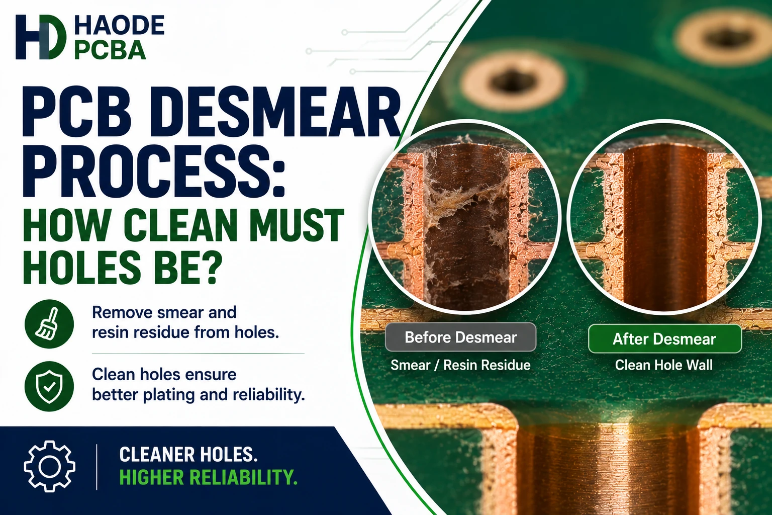
The PCB desmear process removes heat-smeared resin, drilling debris, and other contamination from drilled hole walls before metallization. A hole is clean enough only when the process exposes the required inner-layer copper, leaves a plateable dielectric surface, and produces an interconnect that survives the specified thermal and reliability tests.
Process time alone cannot prove this result. Likewise, a clean-looking hole entrance does not confirm that the full hole depth or every inner-layer interface is clean.
Therefore, buyers should evaluate desmear as a material-specific interconnect process—not as a generic cleaning step.
What Is the PCB Desmear Process?
Mechanical drilling generates friction and heat. As the drill passes through the laminate, softened resin and fine debris can spread across the hole wall and exposed inner-layer copper.
This contamination is commonly called drill smear or resin smear.
If the manufacturer plates over that barrier, the new copper may not bond correctly to the inner-layer copper. Consequently, the PCB can develop PCB interconnect defects during soldering, thermal cycling, or field operation.
A typical plated-through-hole sequence includes:
- Mechanical drilling
- Debris removal
- Desmear or controlled etchback
- Neutralization and rinsing
- Hole-wall conditioning
- Catalyst application
- Electroless copper deposition
- Electrolytic copper plating
Each stage supports the next one. For example, effective desmear cannot compensate for severe drill damage. Similarly, good electroless copper chemistry cannot create a strong interconnect over contaminated inner-layer copper.
NASA’s Printed Circuit Board Inspection and Quality Control material identifies resin-smear removal and hole-wall preparation as critical operations before hole plating.
PCB Desmear Process vs. PCB Etchback
Desmear and etchback are related, but they do not always describe the same manufacturing objective.
| Process | Primary Purpose | Typical Result | Main Risk |
|---|---|---|---|
| Desmear | Remove resin smear and drilling debris | Clean exposed inner-layer copper and plateable hole walls | Residue remains if treatment is insufficient |
| Etchback | Deliberately remove a controlled amount of dielectric | Additional inner-layer copper becomes exposed | Excessive removal changes hole geometry |
| Cleaning And Rinsing | Remove loose debris and chemical residues | Clean surface for the next treatment | Trapped residues contaminate metallization |
| Conditioning | Prepare the dielectric for activation and copper deposition | More uniform catalyst and copper coverage | Poor conditioning contributes to skips or weak adhesion |
A fabrication drawing may require desmear without specifying a measurable etchback distance. Another design may require positive etchback to expose more of the inner-layer copper edge.
Therefore, buyers should not use the terms interchangeably without defining the intended result.
Moreover, no single etchback amount suits every laminate, hole size, copper construction, and reliability class. The applicable drawing and specification must control the acceptance requirement.
Why Do Drilled PCB Holes Develop Resin Smear?
Drill smear develops when heat, mechanical pressure, and chip movement transfer resin-containing material across the hole wall.
Several conditions can increase the risk:
- Worn drill bits
- Excessive drill hits
- Incorrect spindle speed
- Unsuitable infeed or retract rate
- Poor chip evacuation
- Inappropriate entry or backup material
- High board thickness
- Small drill diameter
- High laminate glass content
- Inorganic fillers
- Difficult resin chemistry
- Excessive panel stack height
High-aspect-ratio holes create an additional challenge because chemistry, plasma, rinsing, and debris removal must work through a deep and narrow structure.
As a result, the manufacturer should review the PCB aspect ratio together with drilling and desmear capability. A process that works for a 1.6 mm board with a large hole may not work equally well for a thick board with a small finished hole.
However, aspect ratio alone does not prove the root cause. The supplier must also evaluate drill condition, laminate type, solution exchange, plasma uniformity, rinsing, and subsequent metallization.
How Does Chemical PCB Desmear Work?
Chemical desmear commonly uses a sequence that conditions or swells the resin, oxidizes and removes resin material, neutralizes reaction products, and thoroughly rinses the hole.
Alkaline permanganate systems are widely associated with this process. However, suppliers must control the complete line rather than focusing only on the permanganate bath.
Important variables include:
- Laminate compatibility
- Bath concentration
- Solution temperature
- Treatment time
- Chemical loading
- Agitation
- Solution exchange inside small holes
- Neutralization effectiveness
- Rinse-water quality
- Contamination level
- Maintenance and replenishment history
Chemical desmear can process many conventional rigid PCB materials efficiently. Nevertheless, removal rate depends strongly on the resin system.
Therefore, increasing treatment time without material data may create a new problem instead of solving the original one.
When Should a Manufacturer Use Plasma Desmear?
Plasma desmear uses controlled gases, pressure, radio-frequency energy, and exposure time to modify or remove material from drilled hole walls.
Manufacturers may consider plasma when:
- The laminate resists conventional wet chemistry
- Small or deep holes limit chemical exchange
- The construction contains polyimide
- The board contains mixed material systems
- Inorganic filler complicates residue removal
- A rigid-flex construction needs specialized treatment
- Chemical processing alone does not produce a stable interface
Key plasma variables include:
- Gas composition
- Chamber pressure
- RF power
- Exposure time
- Load size
- Panel spacing
- Hole geometry
- Material position within the load
- Chamber condition
However, plasma is not automatically superior to chemical desmear. The process can still produce nonuniform treatment, insufficient debris removal, excessive resin removal, or material damage if the supplier uses the wrong parameters.
Isola’s technical paper on interconnect defects and desmear control emphasizes material-dependent removal, load uniformity, rinsing, chemistry control, and the risks of both insufficient and excessive desmear.
Should a PCB Use Chemical Desmear, Plasma, or Both?
The laminate and via structure should determine the choice.
| Board Condition | Chemical Desmear | Plasma Desmear | Combined Process |
|---|---|---|---|
| Conventional FR-4 Through Holes | Commonly Suitable | Sometimes Used | Usually Unnecessary |
| Filled Low-Loss Laminate | Requires Qualification | Often Considered | May Improve Process Margin |
| Polyimide Or Rigid-Flex | Chemistry Dependent | Frequently Considered | Application Dependent |
| Deep, Small Through Holes | Solution Exchange Must Be Verified | Uniformity Must Be Verified | May Be Appropriate |
| Mixed Dielectric Construction | Separate Material Responses Matter | Gas Compatibility Matters | Often Requires Trials |
| PTFE-Based Material | Standard FR-4 Chemistry May Be Unsuitable | Specialized Treatment May Be Needed | Supplier Review Required |
The correct answer cannot come from the material category alone. Two nominally similar low-loss laminates may contain different resins, fillers, copper treatments, or reinforcement structures.
Accordingly, the fabricator should qualify the selected drilling and desmear process for the exact approved material family.
How Clean Must the PCB Desmear Process Leave a Hole?
The PCB desmear process must remove contamination that blocks metallization or weakens the inner-layer connection. At the same time, it must preserve the hole geometry and laminate structure.
A satisfactory hole should show:
- No residual smear over required inner-layer copper interfaces
- No loose drilling debris
- Suitable dielectric surface preparation
- Continuous metallization coverage
- Acceptable inner-layer copper exposure
- No excessive glass-fiber protrusion
- No damaging resin removal
- No harmful chemical residue
- No abnormal inner-layer copper attack
- Stable performance after required thermal stress
This definition matters because “clean” is not merely a visual description. Instead, it connects a physical interface with its electrical and thermal performance.
The Global Electronics Association’s PCB Fabrication: Troubleshooting & Defect Analysis course also treats drilling, desmear, etchback, material effects, and PTH metallization as connected process areas.
What Happens When Desmear Is Insufficient?
Insufficient desmear can leave resin, filler, glass debris, or reaction products on the hole wall.
Possible results include:
- Inner-layer separation
- Electroless copper skips
- Local plating discontinuity
- Weak copper adhesion
- Intermittent electrical resistance
- Thermal-stress failures
- Assembly-related opens
- Early field failures
Residual smear may contribute to Type I interconnect separation because it prevents direct bonding between the exposed inner-layer copper and the deposited copper.
In other cases, contamination can contribute to PCB plating voids. However, investigators should not label every void as a desmear problem. Catalyst coverage, electroless copper activity, air entrapment, solution exchange, contamination, and electrolytic plating can produce similar symptoms.
Likewise, PCB hole wall pull-away may involve laminate adhesion, moisture, thermal stress, or hole-wall preparation. The laboratory must identify the actual interface before assigning the cause.
Can the PCB Desmear Process Be Too Aggressive?
Yes. More resin removal does not always create a stronger interconnect.
Excessive desmear or etchback may cause:
- Excessive resin removal
- Glass-fiber protrusion
- Rough or irregular hole walls
- Wicking paths
- Changed dielectric clearance
- Excessive inner-layer copper exposure
- Copper attack
- Difficult rinsing
- Entrapped chemical residue
- Poor hole-wall adhesion
- Reduced process consistency
Moreover, aggressive processing can complicate the interpretation of PCB resin recession. Desmear removes material during fabrication, while resin recession describes dielectric movement or contraction relative to nearby copper. Investigators must distinguish intentional processing geometry from later thermal or material behavior.
Excessive treatment can also weaken the overall hole structure. Nevertheless, a PCB barrel crack usually requires a broader review of copper thickness, plating quality, laminate expansion, hole geometry, and thermal exposure.
Therefore, the process window must balance complete contamination removal with controlled material preservation.
Why Must Desmear Match the Laminate?
Modern laminate names do not fully describe their behavior during drilling and desmear.
High-Tg FR-4, low-Dk/Df materials, filled resin systems, polyimide, PTFE-based laminates, and rigid-flex materials can respond differently to the same chemical or plasma recipe.
For example, filler may:
- Change drilling heat generation
- Alter chip formation
- Remain embedded on exposed copper
- Resist conventional resin-removal chemistry
- Affect hole-wall texture
- Complicate elemental analysis
Qnity’s technical discussion of inner-layer copper reliability explains that drilling can leave resin-containing debris on inner-layer copper. It also notes that filled high-speed and high-Tg materials require drilling and desmear evaluation because unremoved filler can remain at the copper interface.
Consequently, an approved material substitution may require renewed process qualification. A supplier should not assume that two “equivalent” laminate data sheets guarantee identical drilling and desmear behavior.
How Can a Supplier Verify PCB Desmear Quality?
No single inspection method proves every aspect of desmear quality.
| Evidence | What It Can Show | What It Cannot Prove Alone |
|---|---|---|
| Chemical Bath Records | The line operated within defined control limits | Every hole wall was clean |
| Plasma Process Log | Gas, pressure, power, time, and load settings | Uniform treatment through every hole |
| Weight-Loss Data | Relative material removal under controlled conditions | Clean inner-layer copper interfaces |
| Optical Microsection | Sampled hole geometry and visible interfaces | Every production hole is defect-free |
| SEM Examination | High-resolution surface or interface morphology | The full production process cause |
| EDS Or XPS Analysis | Elements present in a sampled defect area | Whether residue affects every board |
| Electrical Test | Continuity at the time of testing | Interfacial adhesion or thermal durability |
| Post-Thermal Microsection | Sampled physical condition after stress | Full-lot performance |
| Resistance-Monitored Cycling | Interconnect behavior during thermal exposure | Exact defect chemistry without analysis |
A proper PCB microsection remains one of the most useful production tools. However, the coupon must represent the critical hole structure.
Therefore, the inspection plan should consider:
- Smallest drilled hole
- Highest aspect ratio
- Critical inner-layer connection
- Panel edge and center positions
- Different laminate regions
- Different drill tools or hit ranges
- Pre- and post-thermal specimens
The laboratory should initially inspect a polished, unetched section when confirming suspected separation. Etching can reveal useful grain information, but it may also make some interfaces appear more prominent.
When Is Advanced Surface Analysis Necessary?
Routine production does not require SEM, EDS, or XPS analysis for every PCB lot.
However, advanced analysis can add value when:
- Optical inspection cannot identify the residue
- Defects recur on one material family
- Filled laminate is involved
- The supplier suspects inorganic contamination
- Desmear adjustments do not correct the failure
- Inner-layer separation appears only after thermal stress
- Similar-looking failures may have different causes
For example, EDS can identify elements associated with certain fillers or process residues at a sampled location. Nevertheless, finding silicon, aluminum, calcium, manganese, or another element does not automatically prove the complete failure mechanism.
The investigator must compare the finding with drilling history, desmear records, plating data, control samples, and interface location.
A structured PCBA failure analysis should separate observations, analytical results, proposed mechanisms, and verified root causes.
How Should Thermal Testing Support Desmear Qualification?
A plated hole may pass room-temperature continuity testing even when its inner-layer interface has weak adhesion.
Thermal exposure expands the laminate in the Z-axis and places stress on the copper interconnection. As a result, an unstable interface may separate during soldering, thermal cycling, or repeated service temperature changes.
Qualification may combine:
- Specified preconditioning
- Solder float or thermal stress
- Assembly-representative reflow cycles
- Post-stress microsectioning
- Interconnect stress testing
- Resistance monitoring during temperature cycling
The test conditions must reflect the applicable product specification and material capability. A fabricator should not invent one severe test and apply it to every design.
Moreover, buyers should compare the qualification temperature with the actual PCB reflow soldering profile. A board may experience multiple lead-free reflow cycles, selective soldering, rework, or other thermal events.
PCB Desmear Troubleshooting Matrix
| Observed Result | Possible Desmear-Related Cause | Evidence to Request |
|---|---|---|
| Separation At Inner-Layer Copper | Residual smear, filler, oxide, or weak metallization bond | Unetched section, SEM/EDS if necessary, process records |
| Isolated Hole-Wall Void | Local debris or poor solution exchange | Multiple sections, hole-size comparison, catalyst and plating data |
| Defects Only in Small Holes | Inadequate exchange or nonuniform plasma exposure | Hole-size distribution, load map, coupon location |
| Glass Bundles Protrude Excessively | Over-aggressive resin removal | Microsection, weight-loss trend, recipe history |
| Residue Appears After Chemical Desmear | Poor neutralization, rinsing, or bath control | Rinse data, chemistry analysis, residue identification |
| Failure Appears After Reflow | Weak interface exposed by thermal stress | Pre- and post-reflow sections, resistance monitoring |
| Defects Follow One Laminate Lot | Material-process interaction | Material certificates, controlled comparison trial |
| Panel Edges Perform Differently | Load, agitation, temperature, or plasma nonuniformity | Panel map and chamber or line loading records |
This matrix narrows the investigation. However, it does not replace physical confirmation of the failure interface.
What Should Buyers Specify for the PCB Desmear Process?
Most buyers should specify the required result and evidence rather than dictating an unverified factory recipe.
A practical fabrication note could state:
Qualify drilling and desmear for each approved laminate family and critical via structure. No residual smear or contamination is permitted at required inner-layer interconnects. Report the desmear or etchback method, representative coupon location, preconditioning, and microsection evidence. Material substitutions require approval and process requalification where applicable.
The final wording must align with the project’s drawing, contractual standard, revision, and reliability class.
The RFQ should also provide:
- Gerber or ODB++ data
- NC drill files
- Approved stackup
- Laminate manufacturer and grade
- Finished board thickness
- Drill and finished-hole sizes
- Via types
- Maximum aspect ratio
- Copper weight by layer
- Inner-layer connection details
- Material substitution restrictions
- Applicable IPC documents and revisions
- Thermal preconditioning requirements
- Microsection sampling requirements
- Reliability or cycling requirements
If a failure already exists, include the affected date code, panel position, hole size, assembly history, and thermal exposure. That information helps the supplier compare the defect with the correct production records.
PCB Desmear Process DFM Checklist
Before releasing a design, confirm the following:
- Has the fabricator reviewed the exact laminate?
- Does the drill size support the board thickness?
- Are the critical aspect ratios manufacturable?
- Does the supplier have a qualified desmear method for the material?
- Does the drawing distinguish desmear from required etchback?
- Are material substitutions controlled?
- Do coupons represent the smallest or most critical holes?
- Will inspection cover both panel-edge and panel-center locations when necessary?
- Does the test plan include appropriate thermal conditioning?
- Can the supplier provide pre- and post-stress microsections?
- Does the failure plan distinguish smear from plating and laminate defects?
- Are acceptance criteria tied to a named specification and revision?
These questions belong in the broader PCB DFM checklist because hole reliability depends on design, material, drilling, cleaning, metallization, and assembly exposure together.
Final PCB Desmear Process Recommendation
The PCB desmear process is successful only when it creates a clean, plateable, and thermally reliable hole—not simply when the production line completes a predefined cycle.
For conventional FR-4, a qualified chemical process may provide consistent results. In contrast, filled low-loss materials, polyimide, PTFE-based laminates, rigid-flex constructions, and high-aspect-ratio holes may require different chemistry, plasma treatment, or a combined process.
Therefore, buyers should ask four questions:
- Was the process qualified for the exact laminate and hole structure?
- What physical evidence shows clean inner-layer interfaces?
- Did representative holes survive the required thermal exposure?
- How does the supplier control material substitutions and process drift?
Clear answers to these questions provide more useful evidence than a generic statement such as “standard desmear applied.”