PCB Board, Also Called A Printed Circuit Board, Circuit Board, PCB Circuit Board, Or Printed Wiring Board, Forms The Base Of Almost Every Electronic Product. It Supports Electronic Components, Builds Electrical Connections, And Helps Signals Move Through Copper Traces In A Controlled Way.
If You Want To Understand How To Make PCB Board, You Need To Look Beyond Simple Board Cutting Or Copper Etching. A Reliable PCB Requires Smart Circuit Design, Accurate PCB Layout, Clean Gerber Files, Proper Material Selection, Controlled Fabrication, Careful Surface Finish, And Final Electrical Testing.
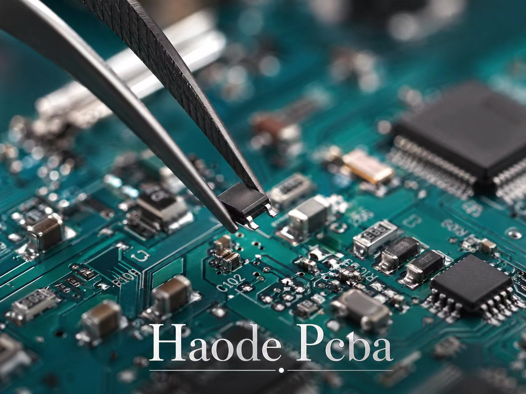
This Guide Explains The Complete PCB Manufacturing Process From Design To Finished Board. It Also Covers Common PCB Keywords Such As PCB Fabrication, PCB Prototype, Copper Trace, Solder Mask, Silkscreen, Via Hole, FR4 PCB, Multilayer PCB, SMT Assembly, And PCBA Manufacturing.
What Is A PCB Board?
A PCB Board Is A Flat Insulating Board With Conductive Copper Paths. These Copper Paths Connect Components Such As Resistors, Capacitors, Diodes, Sensors, Connectors, Microcontrollers, And Integrated Circuits.
A Basic Printed Circuit Board Usually Includes:
- Substrate Material, Such As FR4 Fiberglass, Aluminum, Ceramic, Or Flexible Polyimide
- Copper Layer, Which Forms Traces, Pads, And Power Planes
- Solder Mask, Which Protects Copper And Prevents Solder Bridges
- Silkscreen Layer, Which Marks Component Names, Polarity, Logos, And Test Points
- Surface Finish, Which Protects Exposed Pads And Improves Solderability
In Simple Words, A PCB Turns A Circuit Diagram Into A Physical Electronic Board.
How To Make PCB Board Step By Step
Making A PCB Board Starts With A Digital Design And Ends With A Tested Bare Board Or Fully Assembled PCBA. Each Step Affects Board Quality, Signal Reliability, Soldering Performance, And Long-Term Product Stability.
Step 1: Create The Circuit Schematic
The First Step Is To Create A Circuit Schematic. Engineers Use PCB Design Software To Draw Electrical Connections Between Components.
A Good Schematic Should Include:
- Correct Component Symbols
- Clear Power And Ground Connections
- Accurate Net Names
- Proper Connector Definitions
- Protection Circuits Where Needed
- Test Points For Debugging
This Stage Defines The Logic Of The Circuit. If The Schematic Has Errors, The Finished PCB Board May Not Work Even If The Manufacturing Quality Is Good.
Step 2: Design The PCB Layout
After The Schematic Is Complete, Engineers Convert It Into A PCB Layout. This Layout Shows Where Components Sit On The Board And How Copper Traces Connect Them.
During PCB Layout Design, Engineers Must Control:
- Trace Width
- Trace Spacing
- Via Size
- Pad Size
- Component Clearance
- Power Plane Design
- Ground Plane Design
- Signal Routing
- Impedance Control
- Thermal Relief
- Mounting Holes
- Board Edge Clearance
For High-Speed PCB Design, The Layout Must Also Consider Signal Integrity, Crosstalk, Return Paths, Differential Pairs, And EMI Control. For Power Electronics, The Designer Must Focus On Current Capacity, Copper Thickness, Heat Dissipation, And Safety Spacing.
Step 3: Prepare PCB Manufacturing Files
A PCB Factory Cannot Build A Board From A Picture. It Needs Complete Manufacturing Files. These Files Guide Every Fabrication Step.
Common PCB Production Files Include:
- Gerber Files For Copper Layers, Solder Mask, Silkscreen, And Board Outline
- Drill Files For Vias, Through Holes, And Mounting Holes
- Netlist Files For Electrical Connection Checking
- BOM Files For PCB Assembly Components
- Pick And Place Files For SMT Component Placement
- Stack-Up Details For Multilayer PCB Manufacturing
- Impedance Requirements For High-Speed Boards
Before Sending Files To A PCB Manufacturer, Engineers Usually Run DRC And DFM Checks. These Checks Help Find Spacing Errors, Missing Drill Data, Small Annular Rings, Unclear Board Outlines, And Other Manufacturing Risks.
Step 4: Choose The Right PCB Material
Material Selection Affects Strength, Heat Resistance, Electrical Performance, And Cost.
Common PCB Materials Include:
- FR4 PCB Material For Standard Electronics
- High-Tg FR4 For Higher Temperature Applications
- Aluminum PCB For LED Lighting And Power Modules
- Flexible PCB Material For Bendable Electronics
- Ceramic PCB For High Thermal Conductivity
- Rogers PCB Material For RF And High-Frequency Circuits
For Many Consumer Electronics, Industrial Controllers, IoT Devices, And Power Supplies, FR4 Is The Most Common Choice. However, High-Power, High-Speed, Automotive, Medical, And RF Products May Need More Advanced PCB Laminates.
Step 5: Print The PCB Design Onto Copper Layers
After Material Preparation, The PCB Manufacturer Transfers The Circuit Pattern Onto Copper-Clad Laminate. This Step Often Uses Photoresist And UV Exposure.
The Process Usually Works Like This:
The Factory Cleans The Copper Surface First. Then It Applies A Light-Sensitive Film. After That, The Circuit Pattern Is Exposed Onto The Film. The Exposed Or Unexposed Areas Are Developed, Depending On The Process. This Creates A Protective Pattern For Copper Etching.
This Step Must Be Very Accurate. Poor Imaging Can Cause Broken Traces, Short Circuits, Thin Copper Lines, Or Incorrect Pad Shapes.
Step 6: Etch Away Unwanted Copper
Etching Removes Extra Copper From The Board. The Protected Copper Remains And Becomes The Circuit Pattern.
After Etching, The Board Shows:
- Copper Traces
- Component Pads
- Copper Pours
- Power Planes
- Ground Areas
- Signal Paths
Etching Accuracy Is Very Important For Fine-Pitch Components, High-Density PCB Layouts, BGA Footprints, And High-Speed Circuits.
Step 7: Laminate Layers For Multilayer PCB Boards
For A Single-Layer Or Double-Sided PCB, The Structure Is Simple. However, A Multilayer PCB Board Needs Several Copper And Insulating Layers.
The Factory Stacks Inner Layers, Prepreg, And Copper Foil Together. Then It Uses Heat And Pressure To Laminate Them Into One Solid Board.
Multilayer PCB Manufacturing Supports:
- More Routing Space
- Better Signal Integrity
- Better Power Distribution
- Smaller Board Size
- Higher Component Density
- Stronger EMI Control
Common Multilayer Designs Include 4-Layer PCB, 6-Layer PCB, 8-Layer PCB, And Higher-Layer HDI PCB Boards.
Step 8: Drill Holes And Vias
Drilling Creates Holes For Through-Hole Components, Vias, Mounting Points, And Mechanical Features.
PCB Drilling Can Include:
- Through Holes
- Blind Vias
- Buried Vias
- Microvias
- Countersunk Holes
- Plated Slots
- Non-Plated Holes
Vias Are Especially Important Because They Connect Copper Layers Inside The PCB. If Drilling Accuracy Is Poor, The Via May Not Connect Correctly. This Can Cause Open Circuits Or Reliability Problems.
Step 9: Plate Copper Inside The Holes
After Drilling, The Hole Walls Are Not Conductive. The Factory Adds A Thin Copper Layer Inside The Holes Through Chemical Plating And Electroplating.
Copper Plating Helps Build:
- Conductive Via Walls
- Strong Through-Hole Connections
- Reliable Layer-To-Layer Paths
- Better Mechanical Strength
Good Plating Quality Is Critical For Long-Term Reliability. Weak Plating Can Cause Cracks, Intermittent Failure, Or Electrical Opens Under Heat And Vibration.
Step 10: Apply Solder Mask
The Solder Mask Is The Protective Colored Layer On A PCB Board. Green Is Common, But Black, Blue, Red, White, Purple, And Matte Colors Are Also Available.
Solder Mask Helps To:
- Protect Copper From Oxidation
- Prevent Solder Bridges
- Improve Board Insulation
- Reduce Short Circuit Risk
- Improve PCB Appearance
- Support Stable PCB Assembly
The Factory Leaves Pads, Test Points, And Certain Copper Areas Exposed. These Areas Need Soldering Or Electrical Contact.
Step 11: Add Silkscreen Markings
The Silkscreen Layer Prints Text, Symbols, Logos, Component References, Polarity Marks, Pin Numbers, And Warning Labels Onto The PCB.
Clear Silkscreen Helps During:
- PCB Assembly
- Component Identification
- Repair Work
- Quality Inspection
- Functional Testing
- Field Maintenance
A Good PCB Design Should Keep Silkscreen Clear, Readable, And Away From Solder Pads.
Step 12: Apply Surface Finish
Surface Finish Protects Exposed Copper Pads And Improves Solderability. Without Surface Finish, Copper Can Oxidize Quickly.
Common PCB Surface Finishes Include:
- HASL For Cost-Effective Standard Boards
- Lead-Free HASL For RoHS-Compliant Products
- ENIG For Flat Pads And Fine-Pitch Components
- OSP For Simple And Affordable Production
- Immersion Silver For Good Conductivity
- Immersion Tin For Flat Surface Requirements
- Hard Gold For Edge Connectors And Wear Areas
For BGA, QFN, Fine-Pitch ICs, And High-Reliability PCB Assembly, ENIG Is Often A Strong Choice Because It Provides A Flat And Stable Pad Surface.
Step 13: Route, Score, And Shape The PCB
After Surface Finish, The Factory Cuts The PCB Into Its Final Shape. This Step May Use CNC Routing, V-Scoring, Punching, Or Laser Cutting.
This Process Creates:
- Final Board Outline
- Breakaway Tabs
- Mouse Bites
- Panel Edges
- Slots
- Cutouts
- Connector Openings
For Mass Production, Factories Often Use Panelization. Several PCB Boards Stay Connected In One Panel To Improve SMT Assembly Efficiency.
Step 14: Inspect And Test The PCB Board
A Reliable PCB Manufacturer Tests Each Board Before Shipment. Testing Helps Find Shorts, Opens, Misalignment, Scratches, Missing Copper, Poor Plating, And Other Defects.
Common PCB Quality Checks Include:
- Visual Inspection
- AOI Inspection
- Electrical Testing
- Flying Probe Testing
- Fixture Testing
- Impedance Testing
- Solder Mask Inspection
- Hole Quality Inspection
- Cross-Section Analysis
- Microsection Testing
For Complex Boards, X-Ray Inspection May Also Be Used To Check Hidden Features, BGA Pads, Inner-Layer Alignment, And Plated Through Holes.
Step 15: Assemble Components Into PCBA
If The Project Requires A Finished Electronic Board, The Bare PCB Goes Into PCB Assembly, Also Called PCBA Manufacturing.
The PCBA Process Usually Includes:
- Solder Paste Printing
- SMT Component Placement
- Reflow Soldering
- Through-Hole Insertion
- Wave Soldering Or Selective Soldering
- AOI Inspection
- X-Ray Inspection
- ICT Testing
- Functional Testing
- Final Cleaning And Packaging
At This Stage, The PCB Board Becomes A Working Electronic Assembly.
Common PCB Board Types
Different Applications Need Different PCB Structures. The Main Types Include:
Single-Sided PCB
A Single-Sided PCB Has Copper On One Side Only. It Works Well For Simple Electronics, LED Boards, Toys, Basic Power Modules, And Low-Cost Products.
Double-Sided PCB
A Double-Sided PCB Has Copper On Both Sides. It Supports More Complex Routing And More Compact Designs.
Multilayer PCB
A Multilayer PCB Uses Multiple Copper Layers. It Is Common In Smartphones, Industrial Control Boards, Medical Devices, Servers, Communication Equipment, And Automotive Electronics.
Flexible PCB
A Flexible PCB Can Bend Or Fold. It Is Useful For Wearable Devices, Cameras, Medical Electronics, And Compact Consumer Products.
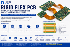
Rigid-Flex PCB
A Rigid-Flex PCB Combines Rigid Board Areas With Flexible Circuits. It Saves Space And Reduces Connector Use In Advanced Electronics.
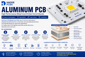
Aluminum PCB
An Aluminum PCB Transfers Heat Better Than Standard FR4. It Is Popular In LED Lighting, Power Supplies, Motor Drivers, And Thermal Control Products.
Important Design Tips Before Making A PCB Board
A Good PCB Board Starts With A Good Design. Before Sending Files To A PCB Factory, Check These Points:
- Keep Trace Width Suitable For Current Load
- Leave Enough Spacing Between Copper Features
- Use A Solid Ground Plane When Possible
- Place Decoupling Capacitors Near IC Power Pins
- Avoid Sharp Trace Angles
- Separate High-Voltage And Low-Voltage Areas
- Control Differential Pair Routing
- Add Test Points For Important Signals
- Choose The Correct Via Size
- Mark Polarity Clearly
- Confirm Hole Sizes And Component Footprints
- Run DRC Before Exporting Gerber Files
- Ask For DFM Review Before Mass Production
These Steps Can Reduce Prototype Errors, Improve Yield, And Lower PCB Manufacturing Cost.
Common Mistakes When Making PCB Boards
Many PCB Problems Start Before Production. Here Are Common Mistakes To Avoid:
- Missing Gerber Layers
- Wrong Drill File Format
- Incorrect Component Footprint
- Poor Grounding Design
- Trace Width Too Small
- Clearance Too Tight
- No Thermal Relief On Pads
- Silkscreen Printed On Pads
- Missing Board Outline
- Wrong Copper Thickness
- Unclear Stack-Up Requirement
- No Impedance Control Notes
- No Test Points
- Poor Panelization Design
Avoiding These Mistakes Makes PCB Prototype Manufacturing Faster And More Reliable.
How To Choose A PCB Manufacturer
A Good PCB Manufacturer Should Do More Than Produce A Cheap Board. It Should Support Stable Quality, Fast Communication, Clear Engineering Review, And Reliable Delivery.
When Choosing A PCB Fabrication Partner, Check:
- PCB Prototype Capability
- Multilayer PCB Manufacturing Experience
- SMT Assembly Capability
- Material Options
- Surface Finish Options
- Quality Control Process
- DFM Support
- Lead Time
- Engineering Communication
- Certifications
- Testing Equipment
- Small Batch And Mass Production Support
For Industrial Electronics, Medical Devices, Automotive Control Boards, Communication Products, And Consumer Electronics, Quality Control Is More Important Than Only Looking At The Lowest PCB Price.
Why PCB Manufacturing Quality Matters
A PCB Board May Look Simple, But It Controls Electrical Performance, Mechanical Strength, Heat Flow, And Product Reliability.
Good PCB Manufacturing Helps Improve:
- Signal Stability
- Power Delivery
- Heat Dissipation
- Solder Joint Strength
- Component Reliability
- Product Lifespan
- Assembly Yield
- Field Performance
- Safety And Compliance
Poor PCB Quality Can Cause Short Circuits, Open Circuits, Weak Soldering, Pad Lifting, Via Failure, Signal Noise, And Product Returns.
Conclusion
Learning How To Make PCB Board Means Understanding The Complete Journey From Circuit Design To Finished PCB Manufacturing. A Reliable PCB Board Requires Accurate Schematic Design, Clean PCB Layout, Correct Gerber Files, Suitable Materials, Precise Drilling, Strong Copper Plating, Protective Solder Mask, Stable Surface Finish, And Strict Electrical Testing.
Whether You Need A PCB Prototype, Custom Printed Circuit Board, Multilayer PCB, FR4 PCB, Aluminum PCB, Or Full PCBA Assembly, Every Step Matters. A Well-Made PCB Board Gives Electronic Products Better Performance, Stronger Reliability, And Longer Service Life.
FAQ About How To Make PCB Board
How Do You Make A PCB Board?
You Make A PCB Board By Creating A Circuit Schematic, Designing The PCB Layout, Exporting Gerber Files, Choosing Materials, Etching Copper, Drilling Holes, Plating Vias, Applying Solder Mask, Adding Silkscreen, Finishing Pads, Cutting The Board, And Running Electrical Tests.
What Files Are Needed For PCB Manufacturing?
Most PCB Manufacturers Need Gerber Files, Drill Files, Board Outline Data, Stack-Up Details, And Special Fabrication Notes. For PCB Assembly, They Also Need BOM Files And Pick And Place Files.
What Material Is Commonly Used For PCB Boards?
FR4 Is The Most Common PCB Material. It Offers Good Mechanical Strength, Electrical Insulation, Heat Resistance, And Cost Performance For Many Electronic Products.
What Is The Difference Between PCB And PCBA?
A PCB Is The Bare Printed Circuit Board Without Components. A PCBA Is A Finished PCB Assembly With Components Soldered Onto The Board.
What Is The Best Surface Finish For PCB Boards?
The Best Surface Finish Depends On The Application. HASL Works For Standard Boards. ENIG Is Better For Fine-Pitch Components, BGA Packages, And High-Reliability PCB Assembly. OSP Is Often Used For Cost-Sensitive Production.
Can I Make A PCB Board At Home?
You Can Make A Simple PCB Board At Home With Basic Etching Methods, But Professional PCB Manufacturing Gives Better Accuracy, Plating Quality, Solder Mask, Surface Finish, Multilayer Capability, And Electrical Testing.
Why Is Gerber File Important In PCB Manufacturing?
Gerber Files Show Each PCB Layer, Including Copper Traces, Solder Mask, Silkscreen, And Board Shape. They Act As The Main Blueprint For PCB Fabrication.