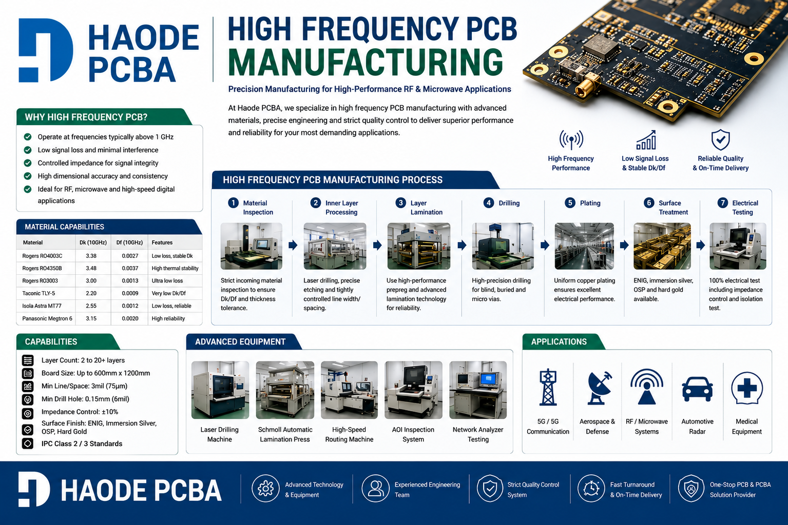
High Frequency PCB Manufacturing Overview
Manufacturing a reliable High Frequency PCB requires more than standard PCB fabrication capabilities. Because RF and microwave circuits are extremely sensitive to material properties, dimensional accuracy, and manufacturing tolerances, every production step must be carefully controlled.
Compared with conventional FR4 PCB manufacturing, high-frequency PCB fabrication requires:
- Advanced low-loss materials
- Precise layer alignment
- Controlled impedance manufacturing
- Strict thickness control
- Specialized drilling processes
- Advanced inspection equipment
A professional High Frequency PCB Manufacturer must have both engineering expertise and advanced production capability to ensure stable electrical performance.
Step 1: Engineering Review And DFM Analysis
Before production begins, engineers review all design files to identify potential manufacturing risks.
Typical files required include:
- Gerber Files
- Drill Files
- BOM Files
- Stackup Information
- Assembly Drawings
- Impedance Requirements
- Material Specifications
During the DFM (Design For Manufacturing) review, engineers analyze:
- Trace width
- Trace spacing
- Layer structure
- Via design
- Copper thickness
- Manufacturing tolerance
- RF routing requirements
Early engineering review helps prevent expensive redesigns and production delays.
Step 2: High Frequency PCB Material Preparation
Material preparation is one of the most critical stages in high-frequency PCB production.
Unlike standard PCB materials, RF laminates require special handling because their electrical properties can be affected by:
- Moisture absorption
- Surface contamination
- Storage conditions
- Temperature changes
Manufacturers must follow strict material management procedures.
Important controls include:
- Proper storage temperature
- Humidity control
- Material traceability
- Batch verification
- Supplier certification review
Reliable manufacturers maintain complete material records to ensure consistency between production batches.
Step 3: Inner Layer Manufacturing
For multilayer High Frequency PCB designs, inner layer fabrication begins with copper-clad laminate preparation.
The process includes:
- Cleaning the copper surface
- Photoresist coating
- Circuit image transfer
- UV exposure
- Chemical development
- Copper etching
- Inspection
At this stage, accuracy is extremely important because even small dimensional changes may affect impedance performance.
Step 4: Layer Alignment And Lamination
Lamination is one of the most challenging processes for high-frequency PCB manufacturing.
During lamination, multiple PCB layers are bonded together using heat and pressure.
Manufacturers must carefully control:
- Temperature profile
- Pressure parameters
- Heating rate
- Resin flow
- Layer registration
Incorrect lamination may cause:
- Layer shifting
- Thickness variation
- Dielectric inconsistency
- Impedance deviation
For RF applications, precise dielectric thickness control is essential because it directly influences signal performance.
Step 5: Precision Drilling
High-frequency PCB designs often contain:
- Small vias
- Microvias
- Back drills
- Dense routing structures
Precision drilling helps maintain:
- Signal integrity
- Layer connectivity
- Mechanical reliability
Common drilling technologies include:
Mechanical Drilling
Used for standard through holes and larger vias.
Laser Drilling
Used for:
- Microvias
- HDI structures
- High-density RF designs
Back Drilling
Used to remove unused via stubs that may cause signal reflections.
Step 6: Copper Plating Process
After drilling, the holes must be plated to create electrical connections between layers.
The plating process requires precise control of:
- Copper thickness
- Uniformity
- Hole wall quality
- Surface condition
Poor plating quality may result in:
- Increased resistance
- Signal loss
- Reliability problems
High-frequency applications require consistent copper distribution because current flow is highly sensitive at microwave frequencies.
Step 7: Circuit Pattern Formation
The outer layer circuit pattern is created through imaging and etching processes.
Manufacturers must maintain strict control over:
- Trace width
- Trace spacing
- Line accuracy
- Copper thickness
For high-frequency circuits, even small deviations can influence:
- Characteristic impedance
- Phase performance
- Transmission efficiency
Step 8: Surface Finish Selection For High Frequency PCB
Surface finish affects both solderability and electrical performance.
Common surface finishes include:
ENIG (Electroless Nickel Immersion Gold)
Advantages:
- Excellent flatness
- Good solderability
- Suitable for fine-pitch components
Applications:
- RF modules
- Communication boards
- High-density assemblies
Immersion Silver
Advantages:
- Excellent electrical conductivity
- Lower signal loss
- Suitable for high-frequency applications
Immersion silver is often selected for advanced RF designs where electrical performance is a priority.
OSP
Advantages:
- Low cost
- Good environmental performance
However, it may not be suitable for all high-frequency applications requiring long-term surface protection.
ENIG Vs Immersion Silver For RF PCB
| Feature | ENIG | Immersion Silver |
|---|---|---|
| Electrical Performance | Good | Excellent |
| Surface Flatness | Excellent | Excellent |
| Cost | Higher | Medium |
| Oxidation Resistance | Excellent | Moderate |
| RF Applications | Common | Widely Used |
The correct choice depends on:
- Frequency range
- Assembly requirements
- Storage conditions
- Reliability expectations
Step 9: Solder Mask And Surface Protection
Solder mask application protects copper traces from:
- Oxidation
- Contamination
- Accidental solder bridging
For high-frequency PCB designs, engineers must consider:
- Dielectric impact
- Thickness variation
- Material compatibility
Some RF applications may require special solder mask solutions or controlled openings.
Step 10: Electrical Testing
Electrical testing verifies whether the finished PCB meets design requirements.
Common tests include:
Flying Probe Test
Suitable for:
- Prototype production
- Low-volume manufacturing
It checks:
- Open circuits
- Short circuits
- Connection integrity
Automated Testing
High-volume production often uses dedicated test fixtures for faster inspection.
Impedance Testing
For High Frequency PCB, impedance testing is essential.
Manufacturers verify:
- 50Ω RF traces
- Differential impedance
- Transmission line consistency
Test reports provide customers with confidence that the PCB meets design specifications.
Step 11: Advanced Inspection Process
A professional PCB supplier uses multiple inspection methods.
AOI Inspection
Automated Optical Inspection detects:
- Missing circuits
- Trace defects
- Pattern errors
- Surface problems
X-Ray Inspection
X-Ray inspection is used for:
- Hidden structures
- Internal connections
- Via quality
- BGA assemblies
Microsection Analysis
Microsection testing evaluates:
- Copper thickness
- Hole quality
- Layer bonding
- Material structure
High Frequency PCB Manufacturing Challenges
Manufacturing RF boards involves several challenges.
Material Compatibility
Different laminates require different processing parameters.
Tight Tolerances
Small dimensional changes can affect electrical performance.
Impedance Control
Manufacturers must maintain consistent electrical characteristics.
Thermal Expansion
Material expansion differences can create reliability issues.
Complex Testing
RF performance requires more advanced verification than standard PCBs.
Why Choose An Experienced High Frequency PCB Manufacturer?
Choosing an experienced supplier reduces technical risk.
A qualified manufacturer should provide:
✓ Advanced PCB fabrication capability
✓ RF material experience
✓ Engineering support
✓ DFM analysis
✓ Controlled impedance testing
✓ Quality inspection system
✓ Prototype and mass production support
✓ Global export experience
A manufacturing partner with complete PCB fabrication and PCB assembly capability can simplify your supply chain and reduce communication costs.
High Frequency PCB Manufacturing Summary
A successful High Frequency PCB Manufacturing process depends on precise engineering, advanced materials, strict process control, and professional testing.
From material selection to final inspection, every step influences RF performance, signal integrity, and product reliability.
Working with a qualified High Frequency PCB Supplier ensures your communication, radar, automotive, and aerospace electronics achieve stable performance in demanding environments.