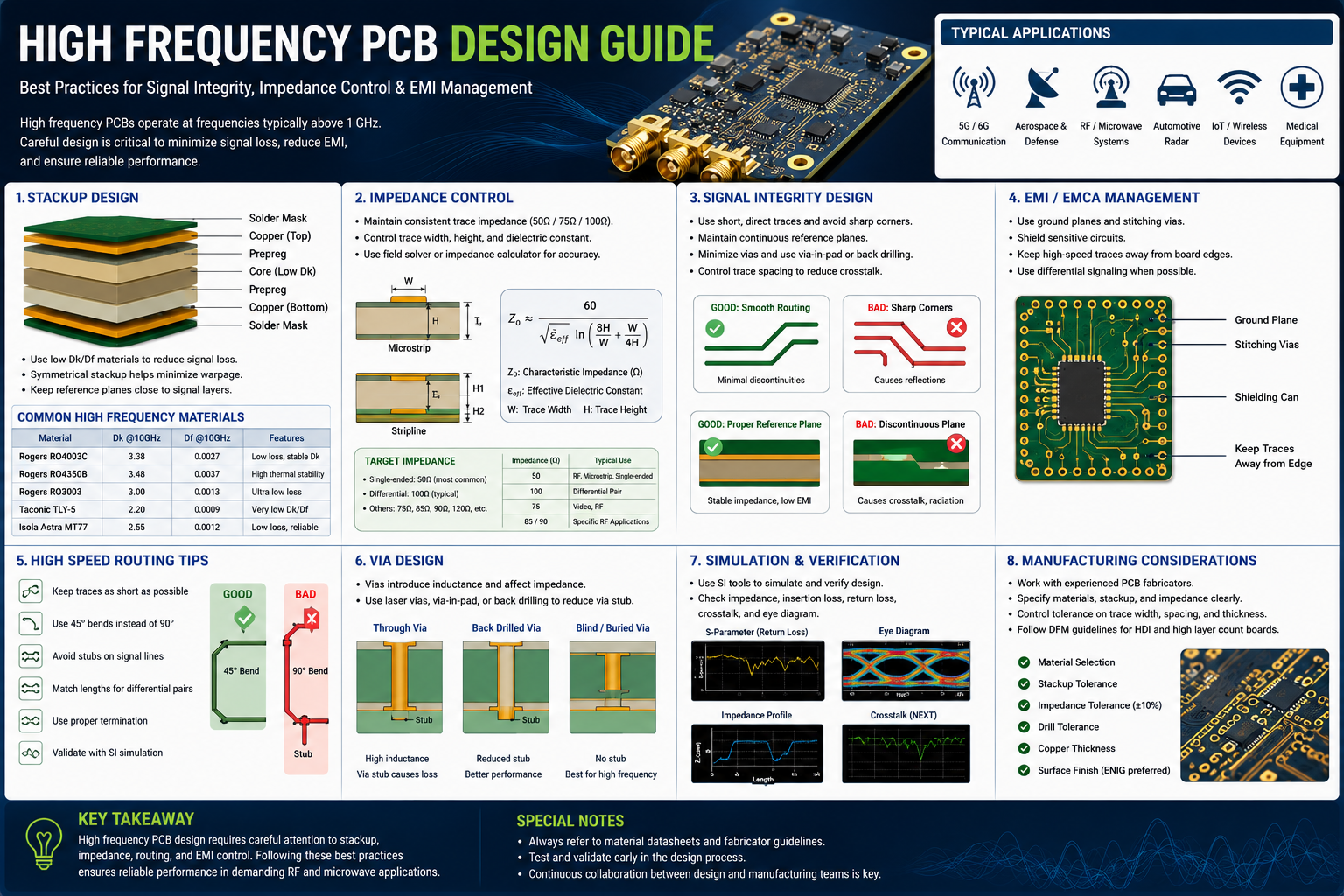
High Frequency PCB Stackup Design
The stackup design is one of the most critical factors affecting the performance of a High Frequency PCB. Unlike standard multilayer PCBs, high-frequency circuit boards require precise control of dielectric thickness, copper layers, reference planes, and transmission line structures.
A well-designed stackup helps engineers achieve:
- Stable impedance control
- Lower signal loss
- Better electromagnetic performance
- Reduced crosstalk
- Improved thermal reliability
For RF and microwave applications, engineers usually place high-frequency signal layers close to reference ground planes. This configuration reduces electromagnetic radiation and creates a more predictable transmission environment.
Common High Frequency PCB Stackup Structures
Microstrip Structure
A microstrip transmission line places the signal trace on the outer layer with a dielectric layer and ground plane underneath.
Advantages:
- Easy fabrication
- Lower manufacturing cost
- Suitable for antennas and RF circuits
Disadvantages:
- More exposed to environmental effects
- Higher radiation loss compared with stripline structures
Stripline Structure
A stripline places the signal layer between two reference planes.
Advantages:
- Excellent impedance control
- Lower electromagnetic radiation
- Better noise immunity
Disadvantages:
- More complex manufacturing process
- Higher fabrication cost
Stripline structures are commonly used in advanced communication equipment, aerospace electronics, and military RF systems.
Grounded Coplanar Waveguide (GCPW)
Grounded coplanar waveguide structures use a signal trace surrounded by ground areas on the same layer.
Advantages:
- Strong EMI control
- Suitable for microwave frequencies
- Excellent RF performance
This structure is frequently applied in:
- 5G modules
- Antenna boards
- Radar systems
- Wireless communication devices
Controlled Impedance In High Frequency PCB Design
Controlled impedance is one of the most important requirements for a High Frequency PCB.
When high-speed signals travel through PCB traces, any impedance mismatch can create signal reflections. These reflections may cause:
- Signal distortion
- Data errors
- Reduced transmission distance
- Communication failure
A PCB manufacturer must accurately control:
- Trace width
- Copper thickness
- Dielectric thickness
- Material Dk value
- Layer spacing
Common impedance requirements include:
| Application | Typical Impedance |
|---|---|
| RF Communication | 50Ω |
| Video Systems | 75Ω |
| USB Differential Signal | 90Ω |
| Ethernet | 100Ω |
| PCIe Interface | 85Ω |
A reliable High Frequency PCB Manufacturer should provide impedance testing reports and maintain strict process control during fabrication.
Understanding Dielectric Constant (Dk)
The dielectric constant, commonly represented as Dk, describes how effectively a PCB material stores electrical energy compared with air.
For high-frequency applications, Dk stability is extremely important because it directly affects:
- Signal propagation speed
- Wavelength
- Impedance
- Phase accuracy
A material with inconsistent Dk values may cause:
- Frequency deviation
- Signal timing problems
- Antenna performance reduction
Therefore, high-frequency materials are selected based on stable Dk performance across the operating frequency range.
Why Dk Stability Matters
A PCB material may have a similar Dk value at low frequencies but behave differently at microwave frequencies.
For example:
A communication system operating at 28 GHz for 5G applications requires much tighter material control than a low-frequency control board.
Small variations in dielectric properties can influence:
- Antenna radiation efficiency
- Beamforming accuracy
- Signal transmission distance
This is why advanced RF designs often use specialized laminates from manufacturers such as Rogers, Taconic, Isola, or Panasonic.
Understanding Dissipation Factor (Df)
The dissipation factor, also called loss tangent (Df), measures how much electrical energy is converted into heat inside the PCB material.
A lower Df means:
- Lower signal attenuation
- Reduced insertion loss
- Better high-frequency performance
High-frequency applications usually require materials with very low Df values.
Typical applications requiring low-loss materials include:
- Microwave communication
- Satellite systems
- Automotive radar
- 5G infrastructure
- High-speed networking equipment
High Frequency PCB Signal Integrity Design
Signal integrity becomes increasingly challenging as frequency increases.
A poorly designed PCB may experience:
- Reflection
- Crosstalk
- Electromagnetic interference
- Signal attenuation
- Timing errors
Engineers improve signal integrity through:
Shorter Signal Paths
Reducing trace length minimizes transmission loss and propagation delay.
Proper Grounding
Continuous ground planes provide stable return paths for high-frequency signals.
Controlled Routing
High-speed traces should maintain consistent spacing and avoid unnecessary bends.
Differential Pair Design
Differential routing improves noise immunity and maintains signal quality.
Common applications include:
- USB
- Ethernet
- PCIe
- High-speed data communication
Copper Roughness And High Frequency Performance
Copper surface roughness is often overlooked but becomes increasingly important at high frequencies.
At higher frequencies, current tends to flow near the conductor surface. This phenomenon is known as the skin effect.
Rough copper surfaces increase the effective transmission path, causing:
- Higher insertion loss
- Increased signal attenuation
- Reduced RF efficiency
For advanced High Frequency PCB designs, manufacturers may use:
- Low-profile copper
- Very low profile copper (VLP)
- Reverse-treated foil (RTF)
These copper technologies improve signal transmission performance.
Skin Effect In High Frequency PCB
The skin effect describes how alternating current concentrates near the outer surface of a conductor as frequency increases.
Because high-frequency signals mainly travel along the copper surface, the quality of copper foil directly affects electrical performance.
Higher frequency applications require careful consideration of:
- Copper thickness
- Copper treatment
- Surface roughness
- Transmission distance
This factor becomes especially important in:
- 77GHz automotive radar PCB
- 5G antenna PCB
- Satellite communication boards
Via Design For High Frequency PCB
Vias provide electrical connections between PCB layers, but improper via design can negatively affect RF performance.
Common issues include:
- Signal reflection
- Additional inductance
- Impedance discontinuity
High-frequency PCB designs often use:
Via Optimization
Reducing unnecessary vias improves signal performance.
Back Drilling
Removing unused via stubs reduces signal reflection at high frequencies.
Via Fence
A row of grounding vias around RF traces helps:
- Reduce EMI
- Improve shielding
- Maintain impedance consistency
EMI And EMC Management
Electromagnetic interference (EMI) is a major concern in high-frequency electronics.
A poorly designed board may generate unwanted electromagnetic radiation or become sensitive to external noise.
Effective EMI control methods include:
- Ground planes
- Shielding structures
- Via fences
- Proper layer arrangement
- Short return paths
- Controlled impedance routing
Good EMC design improves product reliability and helps products pass regulatory testing.
Thermal Management In High Frequency PCB
Although electrical performance is the primary concern, thermal management remains important.
High-frequency systems may generate significant heat because of:
- RF power amplifiers
- High-speed processors
- Power modules
Thermal design methods include:
- Copper thickness optimization
- Thermal vias
- Metal core materials
- Heat dissipation structures
- Proper component placement
A balanced thermal design prevents performance degradation and improves product lifespan.
High Frequency PCB Vs High Speed PCB
Although these terms are often used together, they describe different requirements.
| Feature | High Frequency PCB | High Speed PCB |
| Main Concern | RF signal transmission | Digital data integrity |
| Frequency Range | MHz to GHz | High data rate signals |
| Key Factor | Material loss | Signal timing |
| Materials | Rogers, PTFE, Low-loss laminates | FR4, Megtron, High-speed materials |
| Applications | Radar, RF, 5G | Servers, CPUs, Networking |
Some modern products require both technologies simultaneously, such as 5G base stations and advanced automotive systems.
High Frequency PCB Design Checklist
Before manufacturing, engineers should verify:
✓ Correct laminate selection
✓ Stable Dk and Df values
✓ Controlled impedance requirements
✓ Proper stackup configuration
✓ Signal integrity simulation
✓ EMI prevention strategy
✓ Thermal analysis
✓ Manufacturing capability review
✓ RF testing requirements
Early design verification reduces production failures and unnecessary costs.