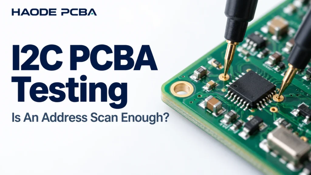
I2C PCBA Testing: Is An Address Scan Enough?
I2C PCBA testing should use an address scan as a communication checkpoint, not as complete functional acceptance. A device acknowledging


I2C PCBA testing should use an address scan as a communication checkpoint, not as complete functional acceptance. A device acknowledging
eMMC replacement should receive production approval only after the proposed device passes a documented review of its package, electrical interface,
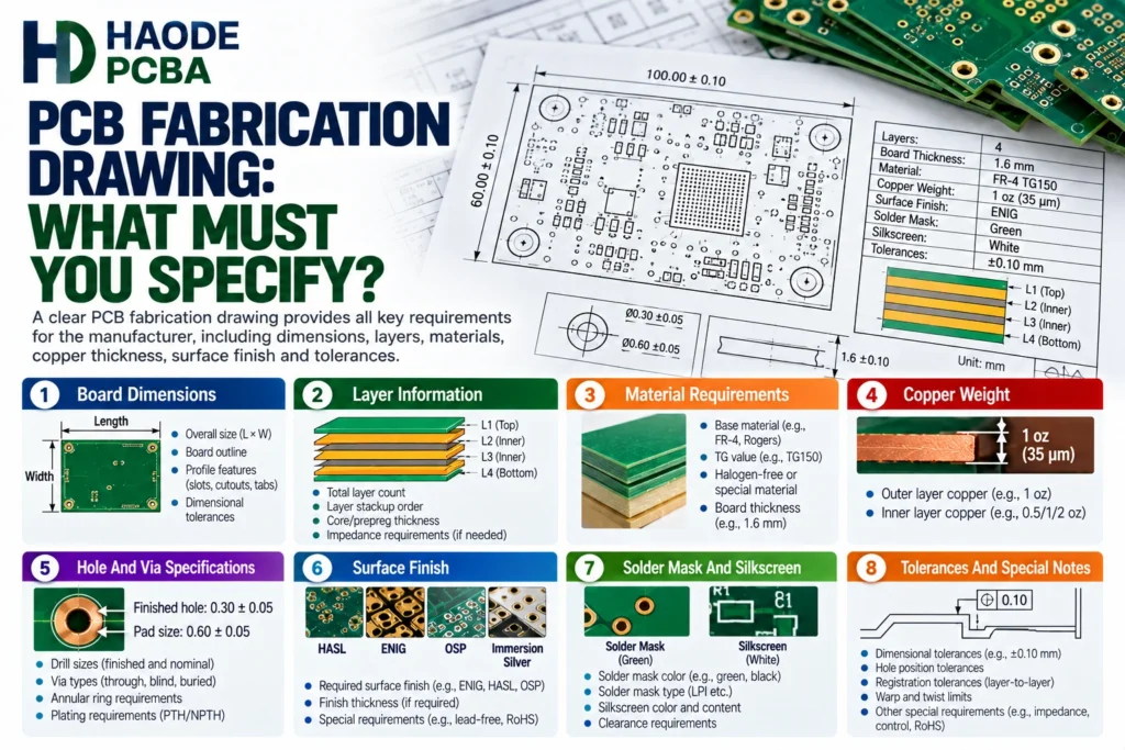
A PCB fabrication drawing defines the physical, material, dimensional, performance, and inspection requirements for an unpopulated printed circuit board. It
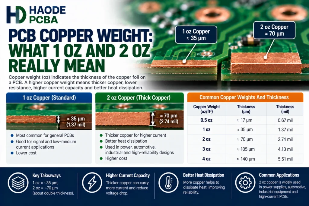
PCB copper weight describes copper mass per unit area, normally in ounces per square foot. It does not directly specify
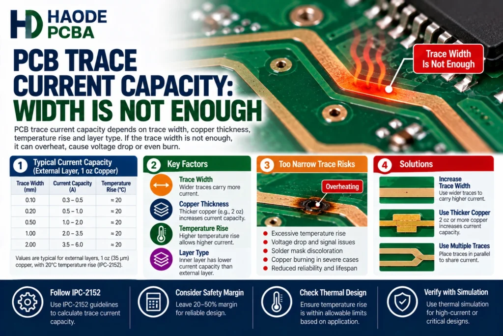
PCB trace current capacity depends on the finished copper cross-section, trace length, permitted temperature rise, surrounding copper, airflow, current duration,
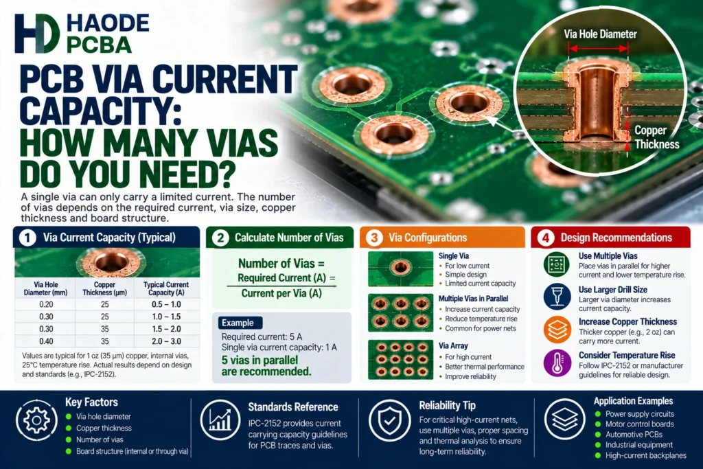
PCB via current capacity cannot be defined by one universal “amps per via” value. It depends on the finished copper
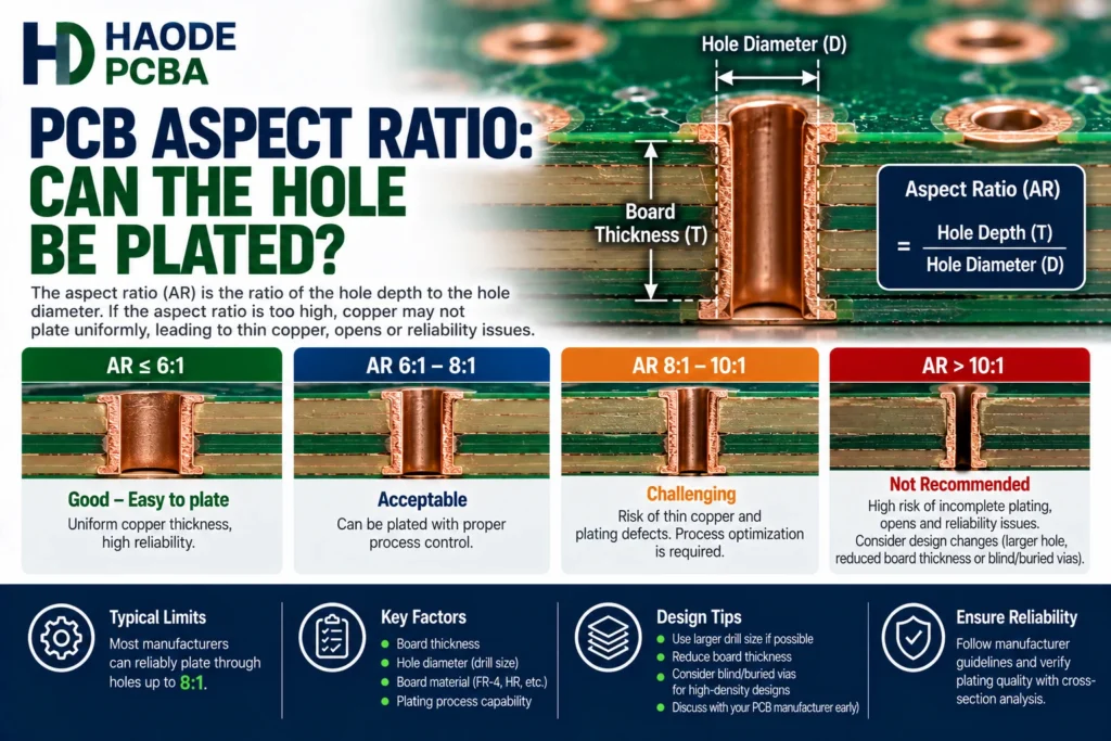
PCB aspect ratio equals the hole depth divided by the drilled-hole diameter. For a plated through hole, manufacturers normally compare

A PCBA annular ring is the copper that remains between the edge of a drilled hole and the edge of

PCB layer registration controls how accurately copper patterns, drilled holes, laser microvias, pads, and plane clearances align across a multilayer
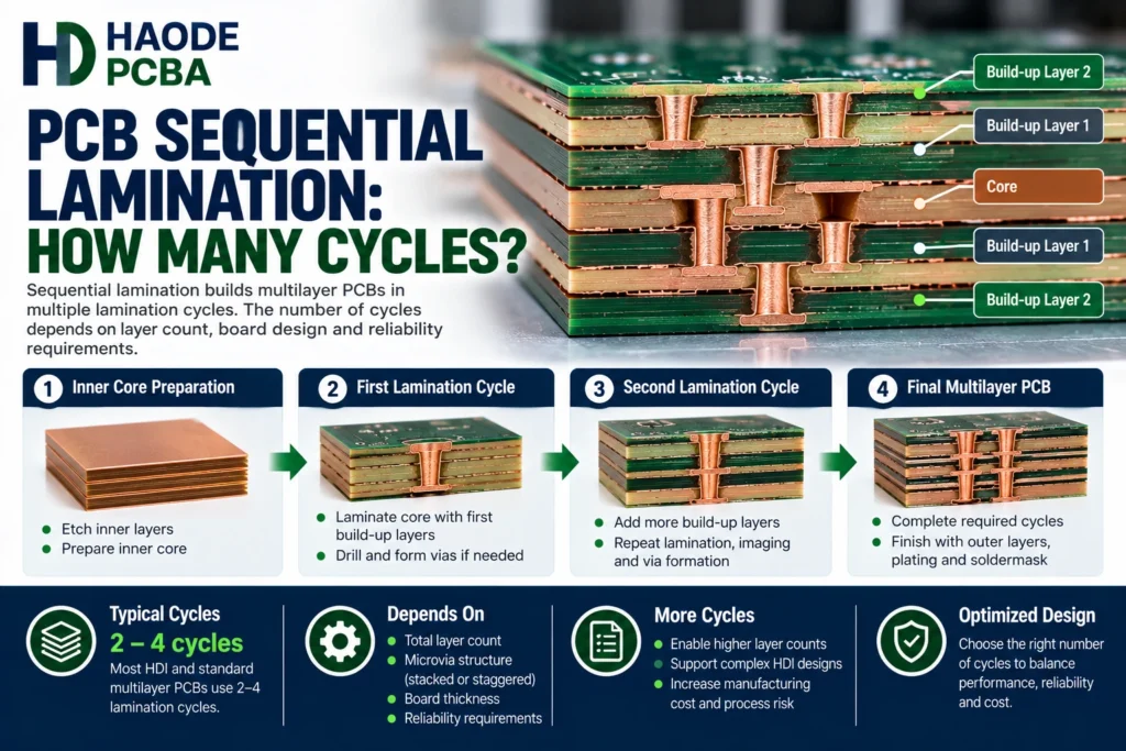
PCB sequential lamination builds a complex PCB through two or more lamination cycles. Manufacturers use it when they must drill,