
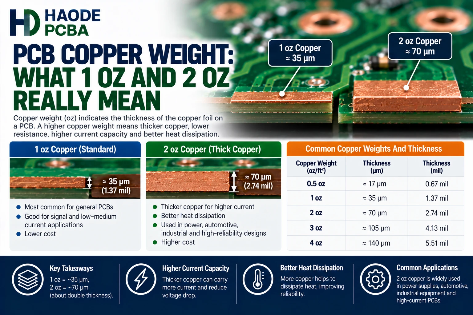
PCB copper weight describes copper mass per unit area, normally in ounces per square foot. It does not directly specify the total copper mass of a circuit board, the exact minimum finished conductor thickness, or how much current a trace can safely carry.
One ounce of copper distributed across one square foot corresponds to approximately 34 µm of theoretical thickness. PCB manufacturers commonly round this value to 35 µm or about 1.4 mil.
However, buyers must still distinguish:
- Starting copper foil
- Finished conductor copper
- External-layer plated copper
- Internal-layer copper
- Hole-wall copper
- Surface finish thickness
- Minimum local copper thickness
Therefore, writing only “1 oz copper” can leave important manufacturing and inspection questions unanswered.
What Does PCB Copper Weight Mean?
PCB copper weight normally uses the unit:
oz/ft²
This unit describes how much copper mass covers one square foot of area. It does not mean that every finished PCB contains one ounce of copper.
For example, a 100 mm × 100 mm board uses only a fraction of one square foot. Moreover, etching removes copper from areas without traces, pads, or planes.
Consequently, the actual copper mass remaining on the finished board depends on:
- Board dimensions
- Copper coverage
- Layer count
- Plane area
- Trace density
- Copper thickness
- Plated features
- Copper-filled structures
IPC-2152 defines copper weight as copper mass per unit area and notes that manufacturers commonly express it in ounces per square foot. The public IPC-2152 table of contents and scope provide the formal terminology.
PCB Copper Weight To Thickness Conversion
The following values represent common industry approximations.
| PCB Copper Weight | Approximate Thickness | Approximate Thickness In Mils |
|---|---|---|
| 0.25 oz | 9 µm | 0.35 mil |
| 0.5 oz | 17–18 µm | 0.7 mil |
| 1 oz | 34–35 µm | 1.35–1.4 mil |
| 1.5 oz | 51–53 µm | 2.0–2.1 mil |
| 2 oz | 68–70 µm | 2.7–2.8 mil |
| 3 oz | 102–105 µm | 4.0–4.1 mil |
| 4 oz | 136–140 µm | 5.4–5.5 mil |
| 6 oz | 204–210 µm | 8.0–8.3 mil |
These values help with preliminary design. Nevertheless, they do not replace the supplier’s finished-copper specification.
Why 1 Oz Is About 34 µm
The theoretical conversion uses copper mass, area, and density:
Thickness = Mass ÷ (Area × Density)
Using:
- One ounce = approximately 28.35 g
- One square foot = approximately 929.03 cm²
- Standard annealed copper density at 20°C = approximately 8.89 g/cm³
The calculation gives a thickness of approximately 34.3 µm.
The NIST copper reference lists 8.89 g/cm³ as the density of standard annealed copper at 20°C.
Manufacturers often round the result to 35 µm. Therefore, 34 µm and 35 µm may both appear in technical literature.
Nominal PCB Copper Weight Versus Finished Copper Thickness
1.Nominal copper weight and minimum finished copper thickness answer different questions.
Nominal Copper Weight
2.Nominal copper weight identifies the intended copper category, such as:
- 0.5 oz
- 1 oz
- 2 oz
- 3 oz
It helps the designer and fabricator select foil, imaging, etching, and plating processes.
Finished Copper Thickness
Finished copper thickness describes the copper remaining on the completed board after relevant processing.
It may include:
- Starting foil
- Pattern plating
- Panel plating
- Etching effects
- Planarization
- Local process variation
Therefore, a drawing that requires electrical resistance, impedance, or current performance should define the relevant finished condition.
Minimum Versus Average Thickness
An average value can hide local thin regions.
For example, five measurements may average 35 µm while one critical conductor measures significantly less. Consequently, buyers should specify whether the requirement applies to:
- Nominal thickness
- Average finished thickness
- Minimum local thickness
- Minimum lot average
- Specific critical areas
The required measurement and acceptance method should match the product risk.
Starting Copper And Finished Copper Are Not The Same
PCB manufacturers build external and internal layers differently. Therefore, identical “1 oz” notes may not describe identical process routes.
Internal-Layer Copper
Internal layers generally begin with copper-clad laminate or copper foil bonded to a core.
The manufacturer then:
- Applies photoresist.
- Images the circuit pattern.
- Develops the resist.
- Etches unwanted copper.
- Strips the remaining resist.
- Laminates the layer into the board.
Internal-layer copper usually does not receive the same full-board pattern plating as external layers.
However, etching and process tolerances can still change the final conductor geometry.
External-Layer Copper
External layers may begin with thinner base copper and then receive additional copper during hole plating and pattern plating.
For example, a manufacturer might use a thinner starting foil and plate the outer conductor to reach the specified finished requirement.
This example does not represent every factory. The actual process depends on:
- Required finished copper
- Trace width and spacing
- Hole copper requirement
- Panel plating or pattern plating
- Surface finish
- Supplier process capability
Therefore, buyers should ask whether a quotation describes starting foil or finished external copper.
PCB Copper Weight By Layer
A multilayer board does not need the same copper weight on every layer.
A controlled stackup table may look like this:
| Layer | Function | Starting Or Finished Copper Requirement |
|---|---|---|
| L1 | Components And Signals | 35 µm Finished |
| L2 | Ground Plane | 35 µm |
| L3 | Power Plane | 70 µm |
| L4 | Power Plane | 70 µm |
| L5 | Ground Plane | 35 µm |
| L6 | Components And Signals | 35 µm Finished |
This construction may support higher-current internal planes while preserving finer surface routing.
However, mixed copper thickness affects:
- Stackup symmetry
- Lamination
- Resin flow
- Copper balance
- Impedance
- Etching
- Drilling
- Warpage
Therefore, the designer should review the complete multilayer PCB stackup rather than selecting each layer independently.
Does 1 Oz Copper Mean 35 µm Everywhere?
No.
The 35 µm value is a nominal industry conversion. It does not guarantee that every point on every finished conductor measures exactly 35 µm.
Variation may come from:
- Foil-manufacturing tolerance
- Copper surface treatment
- Etching
- Panel plating
- Pattern plating
- Current-density distribution
- Panel position
- Copper density
- Planarization
- Measurement method
Moreover, the top and bottom of an etched conductor may have different widths. Therefore, the trace cross-section may not form a perfect rectangle.
For critical designs, calculate electrical performance with minimum finished dimensions rather than nominal CAD geometry.
How PCB Copper Weight Affects Current Capacity
Heavier copper increases conductor cross-sectional area when trace width remains constant.
Therefore:
More Copper Thickness → Lower Resistance → Lower Voltage Drop And Lower (I^2R) Loss
For the same trace width and length, changing from 1 oz to 2 oz copper approximately doubles the cross-sectional area and halves the room-temperature resistance.
However, this does not automatically double the permitted current.
Current capacity also depends on:
- Allowed temperature rise
- Trace length
- Internal or external layer
- Plane proximity
- Airflow
- Ambient temperature
- Enclosure
- Current duration
- Local neckdowns
- Via transitions
- Connector resistance
Our PCB trace current capacity article explains how to calculate resistance, voltage drop, power loss, and thermal risk.
Copper Weight Does Not Fix A Narrow Neckdown
A wide 2 oz copper pour may still connect through:
- A narrow component pad
- Thin thermal-relief spokes
- A small via array
- A connector pin
- A fuse footprint
- A restricted plane section
The narrowest section can dominate resistance and temperature rise. Therefore, review the complete current path.
How PCB Copper Weight Affects Trace Width And Spacing
Thicker copper requires deeper etching. As a result, the etchant must remove more material between adjacent conductors.
This can increase:
- Lateral undercut
- Top-to-bottom width difference
- Minimum spacing
- Minimum manufacturable trace width
- Copper-density sensitivity
- Inspection difficulty
IPC technical research has shown that thicker copper increases the difference between the top and bottom widths of an etched conductor.
Therefore, a factory that produces 0.10 mm trace and space with 0.5 oz copper may not support the same geometry with 3 oz copper.
The PCB etch factor article explains how copper thickness and lateral etching change finished conductor geometry.
PCB Copper Weight And Controlled Impedance
Copper thickness affects controlled impedance because it changes conductor geometry and electromagnetic field distribution.
For a given dielectric structure, thicker copper may require a different trace width to maintain the same target impedance.
Relevant variables include:
- Finished copper thickness
- Finished trace width
- Dielectric thickness
- Dielectric constant
- Solder mask
- Reference-plane position
- Etched sidewall shape
- Surface roughness
Therefore, changing from 1 oz to 2 oz copper after impedance calculations can invalidate the original trace width.
The fabricator should use the actual proposed production stackup and finished copper values when calculating impedance.
Copper Roughness Also Matters
High-profile copper foil can increase insertion loss at high frequencies because current interacts with the conductor surface.
Consequently, high-speed and RF designs may need to specify:
- Foil type
- Roughness category
- Treated side
- Low-profile or very-low-profile copper
- Approved laminate construction
Copper weight alone cannot describe high-frequency conductor performance.
Does Heavier Copper Improve Thermal Performance?
Heavier copper can improve in-plane heat spreading.
For example, a large 2 oz copper plane can spread heat laterally more effectively than a geometrically identical 0.5 oz plane.
However, total PCB thermal performance also depends on:
- Plane area
- Thermal vias
- Dielectric thickness
- Dielectric conductivity
- Component attachment
- Copper distribution
- Airflow
- Heat sinks
- Chassis contact
- Enclosure temperature
Therefore, increasing copper weight may help heat spreading without solving the complete thermal path.
In addition, heavy copper increases board thermal mass. Consequently, the PCB may heat and cool more slowly during soldering and operation.
PCB Copper Weight And Via Plating
Copper weight on a conductor layer does not directly equal plated-hole-wall thickness.
A board may specify:
- 2 oz external finished copper
- 1 oz internal copper
- A separate minimum hole-wall copper requirement
These values require different measurements.
Surface copper may build faster than copper at the center of a deep hole. Therefore, thick external copper does not prove adequate hole copper.
High layer count, small drills, and thick boards make plating distribution more difficult. Our PCB plating uniformity article explains how panel position, hole geometry, current density, and solution movement affect copper deposition.
PCB Copper Weight And Warpage
Copper and laminate respond differently to heat and mechanical stress.
If one side of a board contains substantially more copper than the other, the structure may move unevenly during lamination or reflow.
Risk increases with:
- Asymmetrical copper weights
- Uneven copper coverage
- Thick external copper on one side
- Large local copper pours
- Thin laminates
- Large panel dimensions
- Mixed-material stackups
Therefore, designers should balance both copper thickness and copper coverage around the board centerline.
A mechanically symmetrical stackup can still warp if the copper distribution remains locally unbalanced. The PCB warpage article explains how stackup, panel design, lamination, and reflow interact.
How PCB Copper Weight Affects Soldering
Heavy copper removes heat from component pads more quickly during soldering.
Consequently, the assembly process may require adjustments to:
- Preheat
- Reflow profile
- Soldering-iron power
- Selective-solder parameters
- Wave-solder contact time
- Thermal-relief design
- Hole fill
- Rework method
SMT Reflow
Large copper planes can create thermal differences between low-mass and high-mass regions.
A small passive component may reach soldering temperature quickly, while a connector pad tied to heavy copper heats more slowly.
Therefore, the PCB reflow soldering process should use thermocouples at representative thermal locations.
Through-Hole Soldering
Heavy copper can draw heat away from through-hole joints. This may contribute to:
- Insufficient hole fill
- Cold solder joints
- Long contact time
- Flux degradation
- Laminate overheating
- Difficult rework
Thermal reliefs may improve solderability, but they must still support the operating current.
Does Surface Finish Add To PCB Copper Weight?
Normally, no.
Surface finishes such as:
- ENIG
- ENEPIG
- Immersion silver
- Immersion tin
- OSP
- HASL
protect exposed copper or support soldering. They do not change the specified base copper weight.
HASL adds solder rather than copper. ENIG adds nickel and gold. Therefore, designers should not include these coatings as copper cross-sectional area when calculating current capacity.
Likewise, the thickness of a final finish should remain separate from finished conductor copper in technical documentation.
How Manufacturers Inspect Copper Thickness
Different methods answer different questions.
| Inspection Method | Useful For | Limitation |
|---|---|---|
| Copper-Foil Certificate | Starting foil properties | Does not prove finished conductor thickness |
| Microsection | Finished external, internal, and hole copper | Destructive and sample-based |
| X-Ray Fluorescence | Selected metallic coating measurements | Method suitability depends on layer structure |
| Eddy-Current Measurement | Conductive coating thickness in suitable applications | Requires calibration and suitable geometry |
| Weight Measurement | Material or process control | Does not show local conductor thickness |
| Resistance Measurement | Electrical path verification | Geometry and temperature affect the result |
| Optical Measurement | Trace width and etched profile | Does not alone prove copper thickness |
For a critical multilayer board, microsectioning can measure:
- External conductor thickness
- Internal conductor thickness
- Hole-wall copper
- Copper wrap
- Cap plating
- Etched conductor shape
However, one section represents only a limited sample. Therefore, the inspection plan should define panel locations, layer selection, sample quantity, and acceptance criteria.
What IPC Standards Apply To Copper Thickness?
IPC-4562B addresses metal foils used in printed-board applications. It helps define foil type and material requirements.
IPC-6012F provides qualification and performance requirements for finished rigid printed boards, including conductors, plating, holes, and structural evaluation.
These documents serve different purposes:
- IPC-4562 addresses the metal foil material.
- IPC-6012 addresses the finished rigid board.
- The customer drawing defines project-specific layer copper, tolerances, class, and exceptions.
Therefore, writing “copper per IPC” does not fully define a purchasable requirement.
How PCB Copper Weight Affects Cost
Heavier copper can increase cost through several mechanisms:
- More copper material
- Longer plating time
- Additional plating chemistry
- Slower etching
- Wider spacing requirements
- Lower panel yield
- More difficult impedance control
- Greater copper balancing effort
- Specialized lamination
- Additional inspection
- Longer soldering profiles
However, copper weight alone does not determine total price.
A large two-layer 2 oz board may cost less than a small HDI board with 0.5 oz copper, microvias, sequential lamination, filled vias, and tight impedance tolerances.
Therefore, buyers should compare the full fabrication specification rather than applying a fixed percentage increase for each additional ounce of copper.
How To Specify PCB Copper Weight
The fabrication drawing or stackup table should define copper by layer.
Include:
- Layer number
- Layer function
- Starting foil when relevant
- Minimum finished copper when critical
- External or internal layer
- Copper tolerance
- Foil type when required
- Roughness requirement
- Controlled-impedance requirement
- Heavy-copper areas
- Local copper build-up
- Hole-wall copper requirement
- Surface finish
- Applicable IPC class and revision
- Measurement method
- Sampling requirement
Avoid notes such as:
- Standard copper
- Normal 1 oz PCB
- Heavy copper where needed
- Copper per IPC
These notes leave the supplier to decide requirements that may affect current, impedance, etching, cost, and reliability.
The PCB assembly file requirements should keep the drawing, stackup, Gerber, drill, impedance, and quotation data consistent.
PCB Copper Weight DFM Checklist
Before releasing the PCB, verify:
- Is copper weight defined for every layer?
- Does the note describe starting or finished copper?
- Is minimum finished thickness required?
- Are internal and external requirements separated?
- Does the current calculation use minimum copper?
- Has the trace width been recalculated for actual copper thickness?
- Can the supplier etch the required trace and spacing?
- Has controlled impedance been recalculated?
- Is the copper distribution balanced?
- Is the stackup mechanically symmetrical?
- Can the plating process meet hole-copper requirements?
- Does heavy copper affect soldering?
- Are thermal reliefs electrically adequate?
- Does the board need low-profile foil?
- Is the inspection method defined?
- Are critical layers included in microsection sampling?
- Does every released file use the same copper values?
- Has the supplier completed a PCB DFM review?
What Buyers Should Include In The RFQ
A complete copper-weight RFQ should provide:
- PCB part number and revision
- Layer count
- Board dimensions
- Finished board thickness
- Stackup
- Copper weight by layer
- Minimum finished copper where applicable
- Foil type
- Surface roughness requirement
- Minimum trace and spacing
- Controlled-impedance targets
- Smallest finished hole
- Hole-wall copper requirement
- Via types
- Surface finish
- Maximum operating current
- Thermal requirements
- Soldering process
- Applicable IPC class
- Inspection requirements
- Prototype and production quantities
If the design contains heavy-current paths, identify the actual current and permitted temperature rise rather than asking the supplier to infer them from copper weight.
Include these requirements when requesting a PCB assembly quote.
Frequently Asked Questions About PCB Copper Weight
How Thick Is 1 Oz PCB Copper?
One ounce per square foot corresponds to approximately 34 µm of theoretical thickness. Manufacturers commonly round it to 35 µm or about 1.4 mil.
How Thick Is 2 Oz PCB Copper?
Two-ounce copper corresponds to approximately 68–70 µm or about 2.7–2.8 mil.
Is 1 Oz Copper Enough For A PCB?
It depends on current, trace width, trace length, voltage-drop limit, temperature rise, impedance, etching, and mechanical requirements.
Many general electronic products use 1 oz copper, but this does not make it correct for every design.
Is 2 Oz Copper Better Than 1 Oz?
Two-ounce copper reduces resistance and can improve heat spreading. However, it also increases cost and makes fine trace-and-space etching more difficult.
Therefore, it is better only when the design benefits justify the manufacturing tradeoffs.
Does 2 Oz Copper Carry Twice The Current?
Not automatically. It approximately doubles copper cross-sectional area for the same trace width, but current capacity depends on thermal conditions and acceptable temperature rise.
Is External 1 Oz Copper The Same As Internal 1 Oz Copper?
Not necessarily. External copper may combine base foil and plated copper, while internal copper usually comes mainly from etched foil.
The finished requirements and process routes should be defined separately.
Does Surface Finish Count As Copper Thickness?
No. Surface finish should remain separate from conductor copper. ENIG, HASL, OSP, immersion silver, and immersion tin do not redefine PCB copper weight.
Can Every PCB Factory Make 4 Oz Copper?
Not with every trace width, spacing, board size, and layer count.
Heavy copper requires suitable imaging, plating, etching, lamination, and inspection capability.
How Do You Measure Finished PCB Copper Thickness?
Microsectioning provides direct cross-sectional measurements. Other methods may support process control, but their suitability depends on the feature and layer structure.
Should Copper Weight Appear In The Gerber Files?
Gerber files define copper geometry, not copper thickness. The fabrication drawing, stackup, or controlled manufacturing notes should define copper thickness by layer.
Final Recommendations For PCB Copper Weight
Use these principles when specifying copper:
- Treat ounces per square foot as a mass-per-area designation.
- Use approximately 34–35 µm for preliminary 1 oz calculations.
- Separate starting foil from finished copper.
- Define internal and external layers individually.
- Use minimum finished copper for resistance calculations.
- Do not treat hole copper as equal to surface copper.
- Recalculate impedance after changing copper thickness.
- Review etch factor and minimum spacing.
- Balance copper thickness and coverage.
- Evaluate soldering requirements for heavy copper.
- Define inspection and sampling for critical layers.
- Put all copper requirements in the controlled stackup or drawing.
The most important relationship is:
Copper Weight → Finished Copper Geometry → Resistance, Etching, Impedance, Heat Spreading, And Manufacturing Cost
A precise layer-by-layer specification prevents disputes over whether “1 oz” describes starting foil, nominal conversion, or minimum finished conductor thickness.