Introduction
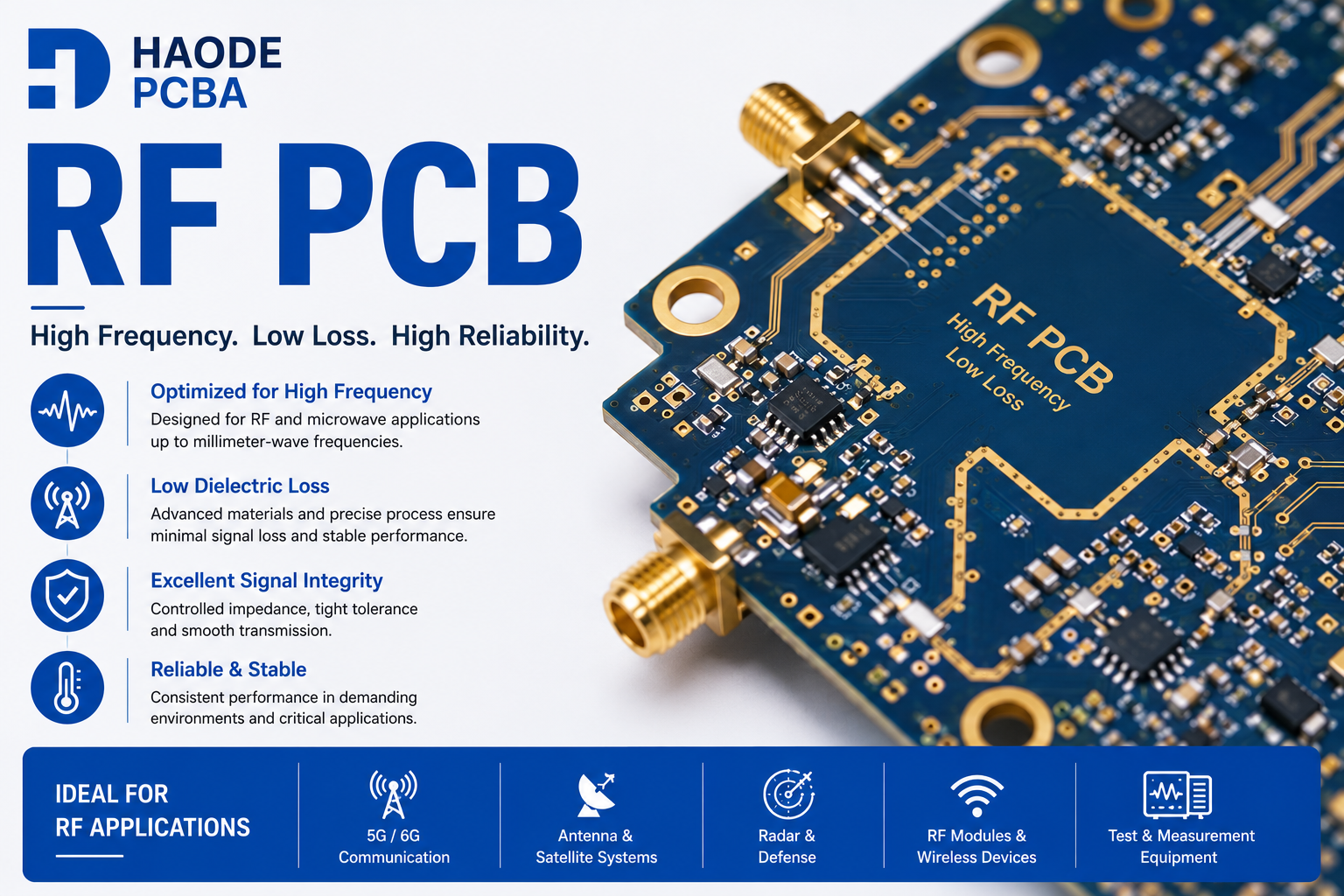
RF PCB technology plays a critical role in modern wireless communication systems by enabling reliable transmission of radio frequency signals. Unlike standard printed circuit boards designed mainly for digital and low-frequency circuits, RF PCBs require specialized materials, precise impedance control, and advanced manufacturing processes to maintain signal integrity.
From 5G networks and automotive radar to satellite communication and IoT devices, RF PCB solutions help engineers achieve stable performance at high frequencies.
Choosing the right RF PCB material and manufacturing partner is essential because even small variations in dielectric properties, trace geometry, or layer structure can significantly affect signal performance.
Quick Answer
An RF PCB (Radio Frequency Printed Circuit Board) is a specialized circuit board designed for transmitting high-frequency electrical signals. RF PCBs use low-loss materials, controlled impedance designs, and optimized layouts to reduce signal loss, electromagnetic interference, and transmission errors in wireless and microwave applications.
What Is An RF PCB?
An RF PCB is a printed circuit board specifically designed for circuits operating in the radio frequency range.
Unlike conventional PCB designs, RF circuits must consider electromagnetic behavior because high-frequency signals travel as electromagnetic waves rather than simple electrical currents.
RF PCB design focuses on:
- Signal transmission efficiency
- Impedance matching
- Low insertion loss
- Noise reduction
- Electromagnetic compatibility
Typical RF frequency ranges include:
- MHz applications
- GHz communication systems
- Microwave frequency bands
- Millimeter-wave applications
RF PCB Vs Standard PCB
Although all RF PCBs are printed circuit boards, not all PCBs can support RF applications.
| Feature | RF PCB | Standard PCB |
|---|---|---|
| Signal Frequency | High Frequency | Low To Medium Frequency |
| Material | Low Loss Materials | FR4 Commonly Used |
| Impedance Control | Strict Requirement | Less Critical |
| Signal Loss | Extremely Important | Less Important |
| Design Complexity | Higher | Lower |
| Applications | Wireless, Radar, Microwave | General Electronics |
RF PCB Materials
Material selection is one of the most important decisions in RF PCBA design.
Common RF PCBA materials include:
Rogers PCB Materials
Rogers is one of the most widely used RF PCBA material suppliers.
Popular materials include:
RO4350B
Suitable for:
- RF amplifiers
- Wireless communication
- Automotive radar
Advantages:
- Low loss
- Easy manufacturing
- Cost-effective
RO4003C
Suitable for:
- RF modules
- GPS systems
- Communication equipment
Advantages:
- Stable dielectric performance
- Excellent dimensional stability
RT5880
Suitable for:
- Microwave circuits
- Satellite systems
- Aerospace applications
Advantages:
- Ultra-low loss
- Excellent high-frequency performance
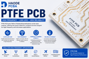
PTFE-Based RF PCB Materials
PTFE materials provide outstanding electrical performance.
Advantages include:
- Extremely low dielectric loss
- Excellent microwave performance
- Stable high-frequency characteristics
Applications:
- Radar
- Aerospace
- Satellite communication
However, PTFE materials require specialized manufacturing processes.
RF PCB Design Considerations
Designing a reliable RF PCB requires careful attention to electrical and mechanical details.
Controlled Impedance Design
Impedance control is one of the most important RF PCB requirements.
Common RF impedance values include:
- 50Ω
- 75Ω
Incorrect impedance may cause:
- Signal reflection
- Power loss
- Communication failure
Manufacturers must control:
- Trace width
- Copper thickness
- Dielectric thickness
- Material properties
RF PCB Stackup Design
The PCB stackup directly affects RF performance.
Important considerations include:
- Signal layer positioning
- Ground plane arrangement
- Dielectric thickness
- Layer spacing
A proper stackup improves:
- Signal integrity
- EMI performance
- Manufacturing consistency
RF Trace Routing
RF traces should be carefully designed.
Recommended practices include:
- Keep traces short
- Maintain constant width
- Avoid unnecessary bends
- Provide continuous ground return paths
- Minimize vias
These methods reduce signal loss and improve RF reliability.
Grounding And Shielding
Good grounding is essential for RF PCBA performance.
Common techniques include:
- Ground planes
- Via fences
- Shielding structures
- Short return paths
Effective grounding reduces:
- EMI
- Crosstalk
- Signal interference
RF PCB Manufacturing Process
Manufacturing RF PCBs requires higher precision compared with standard boards.
The process includes:
Engineering Review
Manufacturers analyze:
- Gerber files
- Stackup requirements
- Material selection
- Impedance specifications
Material Preparation
RF materials require careful handling to maintain electrical consistency.
Lamination
Precise temperature and pressure control are required.
Drilling And Plating
Manufacturers must maintain:
- Hole accuracy
- Copper thickness
- Layer connectivity
Surface Finish
Common finishes include:
- ENIG
- Immersion Silver
- OSP
Testing
RF PCBA testing may include:
- Electrical testing
- Impedance testing
- AOI inspection
- Microsection analysis
RF PCB Applications
1.RF PCBA technology is widely used across many industries.
5G Communication
Applications include:
- Base stations
- Antenna modules
- Wireless communication systems
Automotive Radar
RF PCBs support:
- 24GHz radar
- 77GHz radar
- Autonomous driving sensors
Aerospace And Defense
Applications include:
- Radar systems
- Satellite communication
- Navigation equipment
IoT Devices
RF PCBs enable:
- Wireless sensors
- Smart devices
- Connected products
Medical Electronics
Applications include:
- Imaging systems
- Wireless monitoring equipment
- Diagnostic devices
RF PCB Cost Factors
RF PCBA pricing depends on:
- Material selection
- Layer count
- Board complexity
- Frequency requirements
- Surface finish
- Testing requirements
Compared with standard FR4 PCBs, RF PCBs generally cost more because they require advanced materials and tighter manufacturing control.
How To Choose An RF PCB Manufacturer
A reliable RF PCB Manufacturer should provide:
Material Expertise
Experience with:
- Rogers
- PTFE
- Low-loss laminates
Engineering Support
Including:
- DFM analysis
- Stackup design
- Impedance simulation
Manufacturing Capability
Including:
- High-frequency PCB fabrication
- Precision layer control
- RF testing
Quality Management
Including:
- Material traceability
- Electrical inspection
- Reliability testing
Why Choose Haode PCBA For RF PCB Manufacturing?
Haode PCBA provides professional RF PCB Manufacturing And PCB Assembly Services for global customers.
Our capabilities include:
- Rogers PCB fabrication
- High-frequency PCB manufacturing
- RF material sourcing
- Controlled impedance production
- SMT assembly
- Prototype development
- Mass production
- Quality inspection
With experienced engineers and advanced manufacturing processes, Haode PCBA helps customers build reliable RF products for communication, automotive, industrial, and aerospace applications.
Conclusion
RF PCB technology is essential for modern wireless and high-frequency electronic systems. Compared with standard PCBs, RF PCBs require specialized materials, precise design methods, and advanced manufacturing control.
Selecting the right RF PCB material and experienced manufacturer can significantly improve signal integrity, product reliability, and overall project success.