Introduction
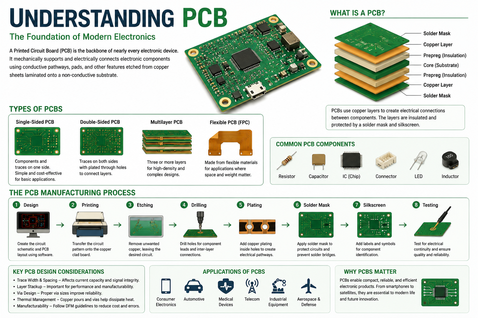
Understanding PCB is the first step to building reliable electronic products. A Printed Circuit Board (PCB) provides the mechanical support and electrical connections for electronic components. Whether you are developing a prototype, designing an IoT device, or preparing for mass production, understanding PCB fundamentals helps reduce manufacturing costs, improve product reliability, and shorten development time.
Quick Answer
A PCB (Printed Circuit Board) is an insulated board with conductive copper traces that electrically connect electronic components. Modern PCBs range from simple single-layer boards to complex HDI, rigid-flex, and high-frequency designs used in automotive, aerospace, industrial control, medical devices, telecommunications, and consumer electronics.
What Is A PCB?
A Printed Circuit Board is the foundation of almost every electronic device. Instead of using individual wires, copper traces are etched onto a laminated substrate to create electrical pathways.
A typical PCB consists of:
- Copper Layers
- Dielectric Material
- Solder Mask
- Silkscreen
- Surface Finish
These layers work together to provide electrical performance, mechanical strength, and long-term reliability.
Why PCBs Are Essential
Without PCBs, modern electronics would be larger, less reliable, and more expensive to manufacture.
PCBs help manufacturers:
- Improve signal integrity
- Reduce assembly errors
- Increase production efficiency
- Lower manufacturing costs
- Support automated SMT assembly
- Improve product consistency
- Enable miniaturization
Main PCB Types
Single-Layer PCB
Suitable for low-cost electronic products with simple circuits.
Applications:
- LED Lighting
- Power Supplies
- Household Appliances
Double-Layer PCB
Uses copper on both sides of the board.
Applications:
- Industrial Controllers
- Consumer Electronics
- Security Equipment
Multilayer PCB
Contains four or more copper layers.
Applications:
- Servers
- Networking Equipment
- Telecommunications
- Medical Electronics
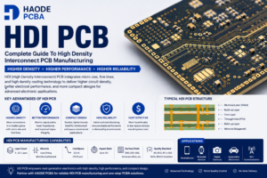
HDI PCB
High Density Interconnect PCBs provide finer traces, microvias, and higher routing density.
Applications:
- Smartphones
- Wearables
- High-Speed Computing
Flexible PCB
Flexible materials allow the circuit to bend repeatedly.
Applications:
- Cameras
- Medical Equipment
- Foldable Devices
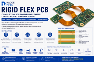
Rigid-Flex PCB
Combines rigid and flexible sections into one board.
Applications:
- Aerospace
- Military Electronics
- Medical Devices
PCB Materials
Material selection directly affects reliability, thermal performance, and signal quality.
Common materials include:
- FR4
- High Tg FR4
- Rogers
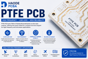
- PTFE
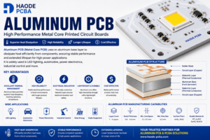
- Aluminum
- Ceramic
- Polyimide
Each material offers different electrical, mechanical, and thermal characteristics.
PCB Manufacturing Process
The manufacturing process typically includes:
- PCB Design Review
- DFM Analysis
- Material Preparation
- Inner Layer Imaging
- Etching
- Lamination
- Drilling
- Copper Plating
- Solder Mask
- Silkscreen Printing
- Surface Finish
- Electrical Testing
- Quality Inspection
- Packaging
Every stage influences final product quality and manufacturing yield.
Surface Finishes
Choosing the correct surface finish improves solderability and reliability.
Common options include:
- ENIG
- HASL
- OSP
- Immersion Silver
- Immersion Tin
- Hard Gold
- ENEPIG
The best choice depends on assembly requirements, component density, and operating environment.
Common PCB Design Mistakes
Many PCB failures originate during the design stage.
Common mistakes include:
- Trace widths that are too narrow
- Poor grounding strategy
- Inadequate thermal relief
- Incorrect hole sizes
- Insufficient spacing
- Ignoring impedance control
- Weak power distribution
- Missing test points
Design reviews before fabrication can significantly reduce rework and manufacturing delays.
PCB Cost Factors
Several factors influence PCB pricing.
These include:
- Layer Count
- Board Size
- Material Type
- Copper Thickness
- Surface Finish
- Drill Count
- Controlled Impedance
- Via Technology
- Quantity
- Delivery Time
Optimizing these factors early often reduces total production costs.
PCB Applications
PCBs are widely used in:
- Automotive Electronics
- Medical Devices
- Aerospace Systems
- Industrial Automation
- Consumer Electronics
- Telecommunications
- Renewable Energy
- Smart Home Products
- IoT Devices
- Security Systems
How To Choose A PCB Manufacturer
Selecting the right manufacturing partner affects quality, lead time, and long-term reliability.
Consider:
- Manufacturing Experience
- IPC Standards Compliance
- ISO Certifications
- DFM Support
- Material Traceability
- Testing Capabilities
- Prototype Services
- Turnkey Assembly
- Engineering Support
- Global Logistics
A supplier that offers both PCB fabrication and PCB assembly can simplify project management and reduce communication costs.
Frequently Asked Questions
What Is The Difference Between PCB And PCBA?
A PCB is the bare circuit board. A PCBA is the completed assembly with electronic components soldered onto the PCB.
Which PCB Material Is Best?
FR4 is suitable for most applications, while Rogers and PTFE are better for high-frequency circuits. Aluminum and ceramic materials perform well in high-power thermal environments.
How Long Does PCB Manufacturing Take?
Prototype boards can often be produced within a few days, while production orders typically require one to three weeks depending on complexity and quantity.
What Files Are Required For PCB Manufacturing?
Most manufacturers require Gerber files, drill files, BOM, pick-and-place files, assembly drawings, and fabrication notes.
Why Is DFM Important?
Design for Manufacturing helps identify potential production issues before fabrication, reducing defects, improving yield, and lowering overall manufacturing costs.
Conclusion
Understanding PCB is essential for designing reliable electronic products and selecting the right manufacturing solution. By learning PCB structures, materials, production processes, and cost drivers, engineers and purchasing teams can improve product quality while reducing development risks.
Why Choose Haode PCBA
Haode PCBA provides one-stop PCB fabrication and PCB assembly services for global customers. Our capabilities include prototype production, low-volume manufacturing, mass production, component sourcing, SMT, through-hole assembly, functional testing, and strict quality inspection. With experienced engineers and advanced manufacturing equipment, we help customers accelerate product development while maintaining consistent quality and competitive pricing.
Call To Action
understanding PCB Looking for a trusted PCB manufacturing partner?