
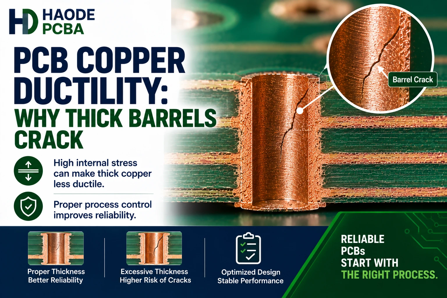
PCB copper ductility describes how much electrodeposited copper can deform before it fractures. It helps explain why a plated through hole can meet its copper-thickness requirement yet still crack during reflow, rework, thermal cycling, or field operation.
However, ductility alone does not determine hole reliability. The PCB designer and manufacturer must also control copper thickness, hole geometry, laminate expansion, plating defects, grain structure, internal stress, and thermal exposure.
Therefore, buyers should treat copper mechanical properties as one part of a complete reliability assessment.
What Is PCB Copper Ductility?
PCB copper ductility is the ability of plated copper to stretch or plastically deform before breaking.
Manufacturers commonly evaluate ductility by measuring elongation on a free-standing electrodeposited copper sample. The test pulls the copper strip until it fractures and calculates how much the gauge length increased.
A simplified expression is:
Elongation (%) = Increase in Gauge Length ÷ Original Gauge Length × 100
For example, if the measured section of a copper strip increases from 50 mm to 56 mm before fracture, its elongation is:
6 ÷ 50 × 100 = 12%
Greater elongation generally indicates that the deposit can accommodate more deformation before it breaks. Nevertheless, a tensile strip and a plated-through-hole barrel do not experience identical constraints.
The strip provides evidence about the plating process. The finished hole still requires product-level verification.
How Do Ductility, Elongation, and Tensile Strength Differ?
These terms describe related but different material properties.
| Property | What It Describes | Typical Reported Unit | Why It Matters |
|---|---|---|---|
| Ductility | Ability to deform before fracture | Often Represented by Elongation | Indicates tolerance to strain |
| Elongation | Increase in length before fracture | Percent | Quantifies deformation in a tensile test |
| Tensile Strength | Maximum tensile stress before failure | MPa Or PSI | Indicates the deposit’s resistance to pulling force |
| Internal Stress | Stress retained within the plated deposit | MPa Or Qualitative Trend | Can promote distortion or cracking |
| Hardness | Resistance to indentation or local deformation | HV Or Other Scale | May help compare deposit conditions |
| Fatigue Resistance | Ability to survive repeated loading | Cycles To Failure | Relates more directly to repeated thermal expansion |
A copper deposit can have high tensile strength but low elongation. In that case, it may resist a large initial force yet fracture after limited deformation.
Conversely, a highly ductile deposit may stretch well but still fail another mechanical requirement if its tensile strength remains too low.
Therefore, “strong copper” and “ductile copper” do not mean the same thing.
What Does IPC Require for PCB Copper Ductility?
IPC-6012F specifies qualification and performance requirements for rigid printed boards. For electrodeposited copper, it identifies a minimum tensile strength of 248 MPa, or 36,000 PSI, and a minimum elongation of 12% when tested under the referenced conditions.
The standard references IPC-TM-650 Method 2.4.18.1 for tensile-strength and elongation testing of in-house plated copper.
However, these numbers require context:
- They apply to electrodeposited copper tested under the specified method.
- They do not replace finished hole-wall copper requirements.
- They do not independently predict cycles to failure.
- Customer specifications may add different or tighter requirements.
- Applicable slash sheets or product standards may impose additional conditions.
- The procurement document should identify the required standard and revision.
The Global Electronics Association’s IPC-TM-650 test method library lists the test methods used to measure copper tensile strength and elongation.
Buyers should avoid writing only “meet IPC ductility.” Instead, the drawing or purchase order should identify the governing document, revision, test method, frequency, and reporting requirement.
How Is Plated Copper Tested?
The manufacturer creates a free-standing copper deposit under controlled plating conditions. The laboratory then prepares test strips from that deposit.
A typical evaluation includes:
- Producing the plated copper sample
- Separating it from the temporary substrate
- Measuring sample width and thickness
- Conditioning the sample as required
- Mounting it in a tensile tester
- Pulling it at the specified rate
- Recording maximum force
- Measuring elongation after fracture
- Calculating tensile strength
- Reporting sample orientation and results
Test details matter because sample thickness, edge quality, orientation, conditioning, pull rate, and measurement technique can affect the result.
A nicked or poorly cut edge can start a premature crack. Likewise, inconsistent sample thickness can distort the tensile-strength calculation.
Consequently, a supplier should report the method and individual measurements rather than issuing a certificate that says only “ductility passed.”
What Does a Copper Tensile Coupon Actually Prove?
A plated copper test strip evaluates the mechanical properties of copper deposited under a defined process condition.
It does not directly test copper inside the customer’s smallest production hole.
| Evidence | What It Can Support | What It Cannot Prove Alone |
|---|---|---|
| Tensile Coupon | Bath deposit strength and elongation | Hole-center thickness or geometry |
| Bath Analysis | Chemistry remained within control limits | Finished copper mechanical properties |
| CVS Or Additive Analysis | Organic additive condition or trend | Thermal life of the PCB |
| Production Microsection | Hole thickness and visible structure | Bulk tensile properties |
| Thermal-Stress Section | Sampled survival after heat exposure | Full-lot fatigue life |
| IST Or Similar Cycling | Resistance stability over repeated cycles | Exact bulk elongation percentage |
| Electrical Test | Circuit continuity at test conditions | Copper ductility or interface strength |
This distinction provides important information for supplier audits.
A tensile coupon can show that the plating bath produced copper with acceptable mechanical properties. However, it cannot show that the board received enough copper at the center of a high-aspect-ratio hole.
That question requires thickness-distribution data such as PCB throwing power.
Why Can Thick Hole Copper Still Crack?
Adequate thickness reduces stress in the copper barrel, but it cannot correct every weakness.
A thick barrel may still crack because of:
- Low copper elongation
- High internal deposit stress
- Brittle or abnormal grain structure
- Plating inclusions
- Voids
- Folds
- Rough drilling damage
- Thin local areas hidden by an acceptable average
- Sharp geometry at the barrel corner
- High laminate Z-axis expansion
- Repeated thermal exposure
- Severe soldering or rework temperature
- Poor inner-layer adhesion
Thus, thickness and mechanical properties must work together.
For example, adding more brittle copper may increase the measured thickness without creating a proportionate improvement in fatigue life.
Likewise, a ductile deposit cannot compensate for a large unplated void or a severely thin hole center.
Our PCB barrel cracks article explains how cracks form at barrel centers, corners, internal-layer interfaces, and other high-stress locations.
How Does the Laminate Stress the Copper Barrel?
PCB laminate and copper expand at different rates when temperature changes.
During heating, the board expands in its Z-axis. The plated hole must stretch with that movement. During cooling, the materials contract again.
One reflow cycle may not fracture a stable hole. However, repeated cycles can accumulate fatigue damage.
Risk increases with:
- Greater board thickness
- Higher laminate Z-axis expansion
- Operation above the material’s glass-transition region
- Small hole diameter
- High aspect ratio
- Thin hole-center copper
- Multiple lead-free reflow cycles
- Rework
- Large temperature ranges
- Repeated field cycling
Therefore, PCB thickness affects more than mechanical fit. It also changes the total Z-axis movement that the plated barrel must accommodate.
The actual PCB reflow soldering profile should support reliability analysis. An oven setpoint alone does not show the temperature reached at the critical hole or component location.
Which Plating Variables Affect PCB Copper Ductility?
PCB copper ductility depends heavily on the acid copper plating process.
Organic Additives
Copper plating baths use proprietary combinations of suppressors, accelerators, levelers, carriers, or brighteners.
These additives control:
- Deposition rate
- Grain structure
- Surface appearance
- Leveling
- Throwing power
- Internal stress
- Mechanical properties
An additive imbalance may produce shiny copper that looks acceptable but has unsuitable mechanical properties.
Therefore, visual appearance cannot replace tensile and elongation testing.
Current Density
Current density influences deposition rate and copper structure.
Excessive current can create burning, roughness, nodules, or abnormal deposits in high-current regions. However, current that is too low may reduce throughput or change additive behavior.
The correct range depends on the chemistry, equipment, loading, and board design.
Bath Temperature
Temperature affects reaction rates, conductivity, and organic additive performance.
A bath may remain close to its nominal temperature yet develop local variation because of poor circulation or excessive loading.
Chloride And Copper Concentration
Chloride supports the function of many acid-copper additive systems. Copper and acid concentrations also influence conductivity, deposition behavior, and distribution.
The supplier must control the complete chemical balance rather than adjusting one component in isolation.
Organic Breakdown Products
Repeated use, anode behavior, current flow, and contamination can create organic breakdown products.
These products may affect deposit stress, ductility, grain structure, and appearance. Consequently, the factory may need filtration, purification, carbon treatment, dummy plating, or controlled bath replacement.
Contamination
Metallic and organic contamination can change deposit properties.
Potential sources include:
- Drag-in from earlier processes
- Poor rinsing
- Anode impurities
- Rack contamination
- Equipment materials
- Maintenance chemicals
- Uncontrolled additions
- Degraded organics
A passing copper-thickness measurement will not reveal every contamination-related mechanical problem.
Does Copper Appearance Predict Ductility?
No. Bright, smooth copper can still have unsuitable elongation, internal stress, or grain structure.
Likewise, a slightly different color or brightness does not automatically indicate unreliable copper.
Visual inspection can identify:
- Burning
- Nodules
- Roughness
- Pits
- Contamination
- Uneven deposition
- Abnormal color
However, it cannot quantify elongation or tensile strength.
The same limitation applies to PCB plating uniformity. Uniform-looking surface copper does not prove uniform hole-center thickness or acceptable mechanical performance.
Therefore, suppliers should use visual inspection as a process signal, not as the final ductility test.
Can Plating Voids Reduce Effective Ductility?
A void does not necessarily change the bulk elongation of the copper bath. Instead, it reduces the effective cross-sectional area and creates a local stress concentration.
The copper surrounding the void must carry more strain. Therefore, cracking may start at that location even when a free-standing tensile coupon passes.
The same principle applies to:
- Pits
- Inclusions
- Folds
- Thin spots
- Rough barrel areas
- Drill gouges
- Copper nodules
- Interface separations
Our PCB plating voids article explains how defect location, size, number, and continuity affect acceptance and reliability.
Thus, a good elongation result does not permit uncontrolled structural defects.
Does Copper Ductility Change After Aging?
It can.
Copper deposits may undergo structural changes after plating, heat exposure, storage, or repeated thermal cycling. Mechanical properties measured immediately after deposition may not perfectly represent the aged condition.
Relevant factors include:
- Self-annealing
- Grain growth
- Residual-stress relaxation
- Thermal conditioning
- Organic inclusion
- Deposit thickness
- Storage time
- Test temperature
Therefore, the report should identify whether the test used:
- As-plated copper
- Room-temperature-aged copper
- Heat-conditioned copper
- Another defined preparation
Comparing values without matching the conditioning method can lead to an incorrect conclusion about process stability.
For critical products, buyers should prioritize the specified test condition and product-level thermal evidence instead of selecting the highest number from unrelated supplier data sheets.
How Can a Factory Verify Thermal Reliability?
A useful verification plan connects plating properties with finished-board behavior.
Review Plating-Coupon Data
Confirm tensile strength, elongation, sample condition, bath identification, and test date.
Measure Critical Holes
Use a PCB microsection to inspect:
- Hole-center copper
- Barrel corners
- Plating folds
- Voids
- Inner-layer interfaces
- Drill damage
- Copper distribution
Apply Representative Thermal Stress
The test should reflect the material, assembly process, reliability class, and procurement requirement.
Inspect After Stress
Compare pre- and post-stress sections. For intermittent defects, resistance monitoring during heating provides stronger evidence than a room-temperature measurement alone.
Use Cycling When Necessary
Automotive, aerospace, medical, industrial, server, telecom, and other demanding products may require repeated thermal cycling or interconnect stress testing.
A complete PCBA environmental testing plan should reflect the product’s actual temperature range and service conditions.
How Should Copper-Related Cracks Be Investigated?
A useful investigation separates bulk copper properties from local product defects.
| Finding | Primary Question | Evidence To Request |
|---|---|---|
| Cracks Across Many Hole Sizes | Is the plated copper mechanically unstable? | Tensile, elongation, bath, and contamination data |
| Cracks Mainly in Small Holes | Is hole-center copper too thin? | Thickness map and throwing-power data |
| Cracks Start at Voids | Did a local discontinuity concentrate stress? | Unetched microsections |
| Cracks Occur Only on Thick Boards | Is Z-axis expansion excessive? | Stackup, TMA, and thermal data |
| Cracks Follow Rework | Was thermal exposure uncontrolled? | Rework temperature and time records |
| One Plating Lot Fails | Did chemistry or additives drift? | Lot-specific bath and coupon data |
| Separation Occurs at Inner Layers | Is this an adhesion defect rather than bulk fracture? | Interface analysis |
| Copper Passes Tensile Testing but Holes Fail | Is the coupon unrepresentative of the product? | Production sections and cycling data |
A structured PCBA failure analysis should document observations before assigning a plating-bath root cause.
What Should Buyers Request From a PCB Supplier?
For products with demanding thermal requirements, request:
- Governing PCB specification and revision
- Copper tensile-strength requirement
- Copper elongation requirement
- Test method
- Sample conditioning
- Testing frequency
- Plating-line traceability
- Minimum finished hole copper
- Critical-hole microsections
- Applicable thermal preconditioning
- Post-stress inspection results
- Material and stackup approval
- Corrective-action evidence when failures occur
A useful purchase note could state:
Electrodeposited copper shall meet the tensile-strength and elongation requirements of the specified PCB performance document and revision. Testing shall use the referenced method and required sample conditioning. Critical plated-through holes shall also meet finished copper-thickness and post-thermal integrity requirements.
The buyer should adapt this note to the actual product specification and contract.
PCB Copper Ductility DFM Checklist
Before approving the PCB, confirm:
- Is the board unusually thick?
- Does it contain small through holes?
- What is the maximum aspect ratio?
- What minimum hole-center copper applies?
- Does the laminate have high Z-axis expansion?
- How many reflow cycles will the assembly experience?
- Is selective soldering or rework expected?
- Does the supplier test in-house plated copper?
- Are tensile strength and elongation both reported?
- Is sample conditioning defined?
- Does the coupon represent the production plating bath?
- Are critical holes microsectioned?
- Does thermal testing represent actual assembly exposure?
- Are bath and lot records traceable?
- Are material substitutions controlled?
These questions should become part of the project’s PCB DFM checklist before the design reaches volume production.
Final PCB Copper Ductility Recommendation
PCB copper ductility helps the plated barrel accommodate strain before fracture. Nevertheless, buyers should never evaluate it in isolation.
A reliable plated-through hole requires:
Adequate Copper Thickness + Suitable Elongation And Strength + Low Defect Density + Controlled Hole Geometry + Compatible Laminate Expansion + Verified Thermal Performance
For IPC-6012F rigid-board production, electrodeposited copper requirements include at least 248 MPa tensile strength and 12% elongation under the referenced test conditions. However, those values remain process-property requirements—not a guarantee that every finished hole will survive its intended life.
Therefore, the strongest supplier evidence combines:
- Traceable plating-bath control
- Compliant copper tensile and elongation results
- Representative hole-wall measurements
- Pre- and post-thermal microsections
- Cycling data for high-risk products
This combination explains why the copper is expected to survive instead of relying on thickness, appearance, or one tensile-coupon result alone.