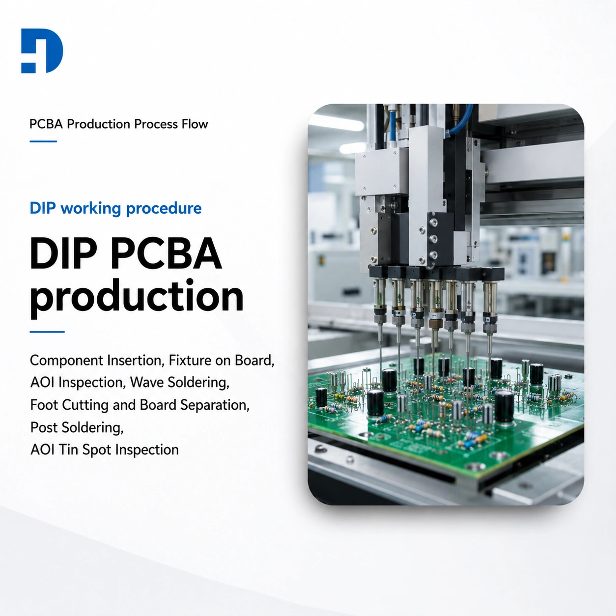
Printed Circuit Boards Are Manufactured By Converting PCB Design Files Into Copper Circuits Through Imaging, Etching, Lamination, Drilling, Plating, Solder Mask, Surface Finish, Testing, And Final Inspection.
What Is PCB Manufacturing?
PCB Manufacturing Is The Process Of Turning A Digital Circuit Design Into A Physical Printed Circuit Board.
The process creates copper traces, pads, vias, holes, solder mask, silkscreen markings, and surface finishes on an insulating base material. The finished bare PCB then supports electronic components during PCB assembly.
What Files Are Needed Before PCB Manufacturing?
A PCB factory usually needs Gerber Files, Drill Files, Netlist Files, BOM Files, And Assembly Drawings.
Gerber or ODB++ files define copper layers, solder mask, silkscreen, board outline, and manufacturing details. Drill files define plated holes, non-plated holes, vias, and mechanical openings.
Step 1: PCB Design Review And DFM Check
Printed Circuit Boards Manufactured starts with a design review.
Engineers check the customer’s files for manufacturability, missing layers, wrong drill data, poor spacing, small annular rings, unclear board outlines, and tolerance conflicts. This step helps prevent production delays and scrap.
Step 2: CAM Engineering
CAM Engineering Converts Design Files Into Factory-Ready Production Data.
The factory creates working films, drill programs, routing data, solder mask data, and inspection references. This step also checks layer order, copper balance, panel size, and design rule compatibility.
Step 3: Raw Material Cutting
The factory cuts copper-clad laminate into production panels.
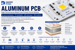
Common base materials include FR-4 fiberglass epoxy, high-Tg FR-4, aluminum substrate, Rogers material, polyimide, and other specialty laminates. The choice depends on thermal, mechanical, electrical, and cost requirements.
Step 4: Inner Layer Imaging
Inner layer imaging transfers the circuit pattern onto copper.
A photosensitive film or photoresist covers the copper surface. Light exposure hardens selected areas, while unexposed areas are developed away. The protected copper becomes the future circuit pattern.
Step 5: Inner Layer Etching
Etching removes unwanted copper from the inner layers.
The protected copper remains as traces, pads, and copper features. The factory controls chemistry, spray pressure, conveyor speed, and copper thickness to keep trace width accurate.
Step 6: Inner Layer AOI Inspection
AOI means Automated Optical Inspection.
The machine compares the manufactured copper pattern with the original design data. It helps find opens, shorts, missing copper, excessive copper, spacing problems, and pattern defects before lamination.
Step 7: Multilayer Stack-Up
A multilayer PCB uses copper cores, prepreg, and copper foil.
The stack-up defines layer order, dielectric thickness, impedance, copper weight, and signal performance. Poor stack-up planning can cause impedance errors, warpage, delamination, and signal integrity problems.
Step 8: Lamination
Lamination bonds PCB layers together with heat and pressure.
Prepreg melts and cures between copper cores and copper foils. This process creates one solid multilayer board. Temperature, pressure, resin flow, and alignment control are critical for reliable PCB fabrication.
Step 9: PCB Drilling
Drilling creates vias, component holes, mounting holes, and mechanical openings.
CNC drilling machines use the drill file to position each hole. For high-density boards, laser drilling may create microvias. Accurate drilling protects annular rings and layer-to-layer connections.
Step 10: Hole Cleaning And Desmear
After drilling, the factory cleans hole walls.
Desmear removes resin residue from drilled holes. Clean hole walls allow copper to bond correctly during plating. Poor desmear can cause weak vias, open circuits, and long-term reliability failures.
Step 11: Electroless Copper Deposition
Electroless copper creates a thin conductive layer inside drilled holes.
This layer allows later electroplating to build stronger copper thickness. It is essential for plated through holes, vias, and multilayer electrical connections.
Step 12: Outer Layer Imaging
Outer layer imaging forms the top and bottom copper patterns.
The process is similar to inner layer imaging. The factory applies photoresist, exposes the outer circuit image, develops the pattern, and prepares the board for copper plating and final etching.
Step 13: Copper Plating
Copper plating increases copper thickness on traces, pads, and hole walls.
This step improves conductivity and creates reliable electrical connections through plated holes. Through-hole copper quality strongly affects current capacity and long-term PCB reliability.
Step 14: Outer Layer Etching
Outer layer etching removes unwanted surface copper.
The remaining copper becomes the final external circuit pattern. The factory must control trace width, spacing, etching time, and copper thickness to avoid shorts and opens.
Step 15: Solder Mask Application
Solder mask protects copper and prevents solder bridges.
It usually gives the PCB its green color, although blue, black, red, white, and other colors are also available. Solder mask leaves pads exposed for soldering components.
Step 16: Silkscreen Printing
Silkscreen adds reference marks, logos, polarity marks, component labels, and warning symbols.
Clear silkscreen helps assembly workers, repair teams, and inspection engineers identify components quickly. It also improves product traceability and service efficiency.
Step 17: Surface Finish
Surface finish protects exposed copper from oxidation.
Common options include HASL, Lead-Free HASL, ENIG, OSP, Immersion Silver, Immersion Tin, And Hard Gold. The right finish depends on solderability, cost, shelf life, flatness, and application requirements.
Step 18: PCB Profiling
Profiling cuts the finished PCB shape from the production panel.
Factories use routing, V-Scoring, or punching. The method depends on board outline, panel design, mechanical tolerance, and customer assembly requirements.
Step 19: Electrical Testing
Electrical testing checks whether every net works correctly.
A flying probe tester or fixture tester verifies continuity and isolation. This step helps detect open circuits, short circuits, wrong connections, and hidden manufacturing defects.
Step 20: Final Inspection And Packaging
Final inspection checks appearance, dimensions, surface finish, solder mask, silkscreen, warpage, hole quality, and shipment condition.
Qualified PCBs are vacuum packed with moisture protection. Packaging helps prevent oxidation, contamination, bending, and handling damage during transportation.
PCB Fabrication Vs PCB Assembly
PCBs Fabrication Makes The Bare Circuit Board.
PCB Assembly Mounts Components Onto The Bare PCB. Assembly may include solder paste printing, SMT placement, reflow soldering, through-hole soldering, AOI, X-Ray inspection, functional testing, and final packing.
Single-Sided PCB Manufacturing
A single-sided PCB has copper on one side only.
It is easier to manufacture and lower in cost. It works well for simple electronics, LED boards, power modules, basic controls, and low-density circuits.
Double-Sided PCB Manufacturing
A double-sided PCB has copper on both sides.
Plated through holes connect the top and bottom layers. It supports higher circuit density than single-sided boards and remains common in consumer electronics, industrial controls, and power products.
Multilayer PCB Manufacturing
A multilayer PCB uses three or more conductive copper layers.
It supports compact routing, controlled impedance, high-speed signals, power planes, ground planes, and complex electronic systems. Its main challenges are stack-up control, lamination, drilling accuracy, and via reliability.
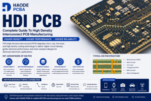
HDI PCB Manufacturing
HDI PCB Manufacturing Uses Fine Lines, Small Vias, Microvias, And Dense Routing.
It is common in smartphones, IoT modules, medical electronics, automotive electronics, and compact embedded systems. HDI boards often require laser drilling, sequential lamination, and strict process control.
What Affects PCB Manufacturing Cost?
PCB cost depends on layer count, board size, material, copper thickness, minimum trace width, minimum spacing, hole size, surface finish, solder mask color, impedance control, testing, and quantity.
More complex specifications increase process steps, inspection time, scrap risk, and production cost.
What Affects PCB Manufacturing Lead Time?
Lead time depends on material availability, layer count, HDI requirements, controlled impedance, special surface finish, tight tolerance, panel utilization, testing method, and production capacity.
Simple two-layer boards can move quickly. Complex multilayer boards need more engineering checks and process control.
Common PCB Manufacturing Defects
Common defects include open circuits, short circuits, under-etching, over-etching, misregistration, drill breakout, plating voids, solder mask misalignment, delamination, warpage, and poor surface finish.
Most defects come from design risk, process control issues, material problems, or incomplete inspection.
How To Improve PCB Manufacturability
Use proper line width, spacing, annular ring, via size, copper balance, solder mask clearance, board outline, and panelization rules.
Send complete Gerber files, drill files, netlist files, BOM files, and assembly drawings. A clear file package helps the PCB manufacturer reduce questions and delays.
What Buyers Should Ask A PCB Manufacturer
Ask about DFM review, material options, copper thickness, controlled impedance, minimum hole size, surface finish, AOI, electrical testing, certificates, traceability, and quality control.
For production orders, also ask about yield control, panel design, packaging, lead time, and repeat-order consistency.
Quick PCB Manufacturing Process Summary
| Step | Purpose |
|---|---|
| DFM Check | Find design risks before production |
| CAM Engineering | Convert files into manufacturing data |
| Imaging | Transfer circuit pattern to copper |
| Etching | Remove unwanted copper |
| AOI | Inspect copper pattern defects |
| Lamination | Bond multilayer structure |
| Drilling | Create vias and holes |
| Plating | Build conductive hole walls |
| Solder Mask | Protect copper and prevent solder bridges |
| Surface Finish | Protect exposed pads |
| Electrical Test | Check opens and shorts |
| Final Inspection | Confirm quality before shipment |
FAQ
How Are Printed Circuit Boards Manufactured?
Printed circuit boards are manufactured by transferring circuit designs onto copper-clad laminate, removing unwanted copper, drilling holes, plating vias, applying solder mask, adding surface finish, testing electrical connections, and inspecting the final board.
What Is The First Step In PCB Manufacturing?
The first step is file review and DFM checking. The factory checks Gerber files, drill files, netlist data, material requirements, dimensions, tolerances, and manufacturing risks before production starts.
Why Is Copper Used In Printed Circuit Boards Manufactured?
Copper is used because it has strong electrical conductivity, good process compatibility, and reliable solderability. It forms traces, pads, planes, and plated through-hole connections inside the PCB.
Why Do PCBs Need Solder Mask?
Solder mask protects copper from oxidation, reduces solder bridges, improves insulation, and makes the board easier to assemble. It also improves visual identification and long-term durability.
Is PCB Manufacturing The Same As PCBA Manufacturing?
No. PCB manufacturing creates the bare printed circuit board. PCBA manufacturing assembles electronic components onto the PCB and turns it into a functional electronic product.