Introduction
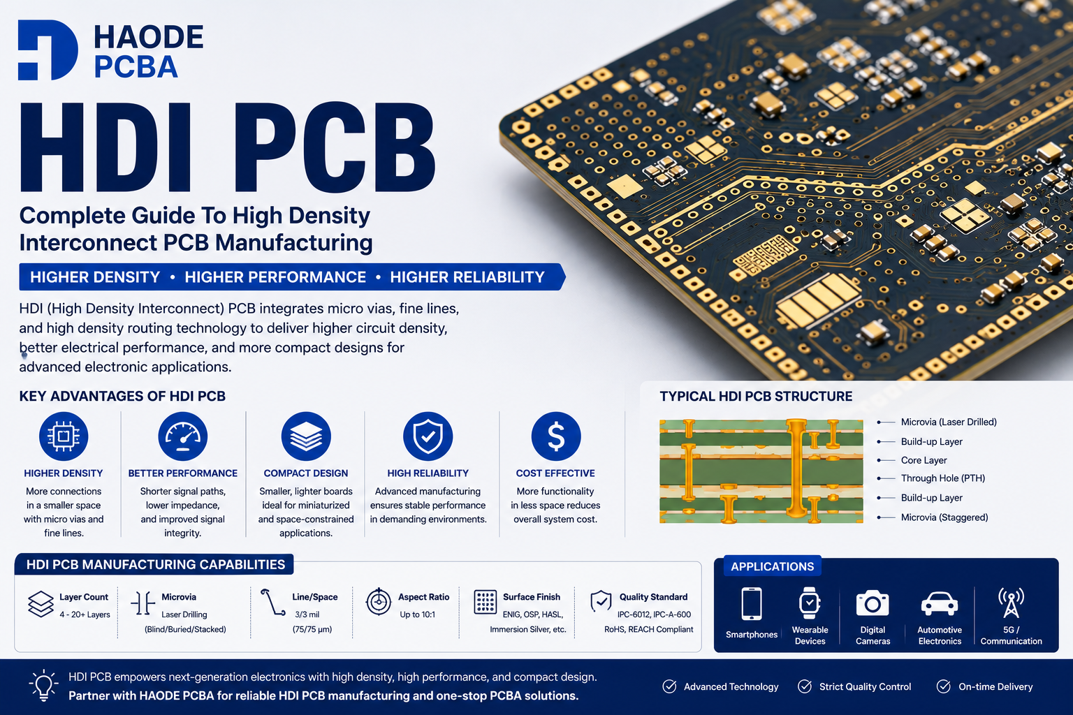
HDI PCB technology has become essential for modern electronic products that require smaller size, higher performance, and increased circuit density. Compared with traditional printed circuit boards, High Density Interconnect (HDI) PCBs use advanced microvia structures, finer traces, and improved layer connectivity to support compact electronic designs.
As electronic devices continue becoming smaller and more powerful, HDI PCB technology enables engineers to integrate more functions into limited space while maintaining reliable electrical performance.
HDI PCBs are widely used in smartphones, medical devices, automotive electronics, aerospace systems, wearable products, and high-performance industrial equipment.
Quick Answer
An HDI PCB (High Density Interconnect PCB) is an advanced circuit board technology that uses microvias, fine lines, and high-density routing structures to achieve greater component density and smaller board sizes. HDI PCBs improve electrical performance, reduce signal path length, and support complex electronic designs.
What Is HDI PCB?
HDI PCB is a type of advanced multilayer PCB designed to increase wiring density through advanced interconnection technology.
Traditional PCBs mainly rely on through-hole vias. However, as electronic products become smaller, traditional vias consume too much board space.
HDI technology solves this problem by using:
- Microvias
- Blind vias
- Buried vias
- Fine trace patterns
- Sequential lamination processes
These technologies allow more circuits to fit into a smaller area.
Why Is HDI PCB Important?
Modern electronics require:
- Smaller dimensions
- Higher processing power
- Faster signal transmission
- More components
- Better reliability
Traditional PCB structures often cannot meet these requirements.
HDI PCB technology provides:
Higher Wiring Density
More circuits can be placed in limited space.
Smaller Product Size
Engineers can reduce PCB dimensions without sacrificing functionality.
Better Electrical Performance
Shorter signal paths reduce:
- Signal delay
- Noise
- Signal loss
Improved Reliability
Advanced via structures provide stronger electrical connections.
HDI PCB Structure
HDI PCB structures are commonly classified according to their build-up technology.
1+N+1 HDI PCB
This is the most common HDI structure.
Features:
- One build-up layer on each side
- Microvias connecting outer layers
- Suitable for compact electronics
Applications:
- Mobile devices
- Consumer electronics
- Industrial equipment
2+N+2 HDI PCB
This structure provides higher routing density.
Features:
- Multiple sequential build-up layers
- More complex interconnections
Applications:
- Advanced communication devices
- High-performance electronics
Any Layer HDI PCB
Any Layer HDI allows microvias between any layers.
Advantages:
- Maximum design flexibility
- Highest routing density
Applications:
- Smartphones
- Advanced computing systems
- High-end electronics
HDI PCB Manufacturing Process
HDI PCB manufacturing requires advanced fabrication technology.
The process includes:
Engineering Review
Before production, engineers review:
- PCB design files
- Layer structure
- Microvia requirements
- Material selection
- Manufacturing capability
DFM analysis helps identify potential production issues.
Inner Layer Manufacturing
The inner layers are produced through:
- Imaging
- Etching
- Inspection
High accuracy is required because small dimensional errors can affect final performance.
Sequential Lamination
Unlike standard PCB manufacturing, HDI PCB production often uses multiple lamination cycles.
This process creates:
- Build-up layers
- Microvia structures
- Advanced interconnections
Precise temperature and pressure control are essential.
Laser Microvia Drilling
Microvias are one of the key technologies behind HDI PCB.
Laser drilling creates extremely small holes that connect adjacent layers.
Benefits include:
- Higher routing density
- Smaller PCB size
- Better electrical performance
Copper Plating
After drilling, microvias require reliable copper plating.
Quality control focuses on:
- Hole wall coverage
- Copper thickness
- Connection reliability
HDI PCBA Design Guidelines
Designing HDI PCBs requires careful planning.
Microvia Design
Microvias should be optimized for:
- Reliability
- Manufacturing capability
- Signal performance
Common considerations include:
- Via diameter
- Via depth
- Via spacing
Stackup Optimization
A proper HDI stackup improves:
- Signal integrity
- Power distribution
- Manufacturing yield
Engineers should balance:
- Layer count
- Cost
- Performance
Fine Line Routing
HDI PCBA designs often use:
- Smaller trace widths
- Smaller spacing
- Higher routing density
Manufacturing capability must match design requirements.
HDI PCBA Vs Standard PCBA
| Feature | HDI PCB | Standard PCB |
|---|---|---|
| Routing Density | Very High | Medium |
| Via Technology | Microvias | Through Holes |
| Size | Smaller | Larger |
| Manufacturing Complexity | Higher | Lower |
| Cost | Higher | Lower |
| Applications | Advanced Electronics | General Products |
HDI PCB Applications
Smartphones And Mobile Devices
HDI technology enables:
- Compact design
- High component density
- Better performance
Medical Electronics
Applications include:
- Portable medical devices
- Diagnostic equipment
- Monitoring systems
Automotive Electronics
Used in:
- Advanced driver assistance systems
- Vehicle control modules
- Smart automotive systems
Aerospace Electronics
Applications include:
- Navigation systems
- Communication equipment
- Avionics
Wearable Devices
HDI PCBA supports:
- Small form factors
- Lightweight designs
- High functionality
HDI PCB Cost Factors
Cost depends on:
- Layer count
- Microvia technology
- Material selection
- Line width and spacing
- Surface finish
- Production volume
Compared with standard PCBs, HDI requires more advanced equipment and manufacturing control.
How To Reduce HDI PCB Cost
Optimize Layer Structure
Avoid unnecessary complexity.
Select Suitable Via Technology
Choose the right balance between:
- Performance
- Reliability
- Cost
Work With An Experienced Manufacturer
A professional HDI PCB manufacturer can improve:
- Manufacturing yield
- Production efficiency
- Cost control
Why Choose Haode PCBA For HDI PCB Manufacturing?
Haode PCBA provides advanced HDI PCB Manufacturing And PCB Assembly Services for customers requiring high-density electronic solutions.
Our capabilities include:
- HDI PCB fabrication
- Multilayer PCB manufacturing
- Microvia technology
- SMT assembly
- Component sourcing
- Prototype production
- Mass production
- Quality inspection
With experienced engineers and advanced manufacturing capabilities, Haode PCBA helps customers develop compact and reliable electronic products.
Conclusion
HDI PCBA technology enables modern electronics to achieve smaller size, higher performance, and greater functionality. Through microvias, fine-line routing, and advanced multilayer structures, HDI PCBs provide solutions for increasingly complex electronic designs.
For smartphones, automotive systems, medical devices, aerospace products, and advanced industrial electronics, choosing an experienced HDI PCB Manufacturer ensures reliable quality, efficient production, and long-term product performance.