
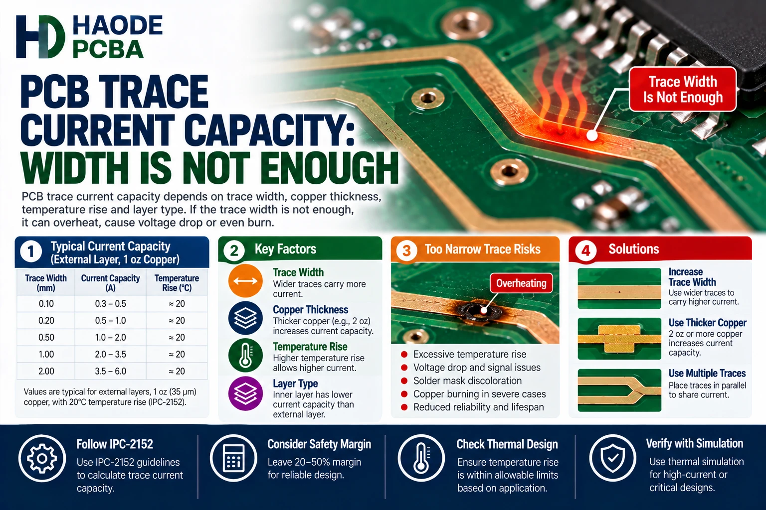
PCB trace current capacity depends on the finished copper cross-section, trace length, permitted temperature rise, surrounding copper, airflow, current duration, and complete power-path geometry. Trace width alone cannot establish a reliable current rating.
A sound design process separates three questions:
- What resistance and voltage drop will the finished trace produce?
- How much (I^2R) heat will that resistance generate?
- Can the PCB and product environment remove that heat without exceeding the temperature limit?
Engineers can calculate the first two. However, the third requires a thermal model, representative measurement, or both.
Therefore, avoid statements such as “a 2 mm trace carries 5 A” unless they also define copper thickness, trace length, acceptable temperature rise, layer position, ambient conditions, and test method.
What Determines PCB Trace Current Capacity?
A copper trace carries current through its cross-sectional area.
The primary geometric inputs are:
- Finished trace width
- Finished copper thickness
- Trace length
- Local neckdowns
- Plane connections
- Thermal-relief geometry
- Via transitions
- Connector and component pads
The operating conditions also matter:
- Continuous current
- Peak current
- Pulse duration
- Duty cycle
- Ambient temperature
- Airflow
- Enclosure temperature
- Nearby heat sources
- Allowed voltage drop
- Allowed conductor temperature
- PCB material and thickness
Consequently, two traces with the same width may have very different current capacities.
For example, a short external trace connected to large copper pours may dissipate heat effectively. In contrast, a long internal trace between warm planes may develop more voltage drop and reach a higher temperature.
How To Calculate PCB Trace Resistance
Calculate the copper cross-sectional area first:
A = W × T
Where:
- A = copper cross-sectional area
- W = finished trace width
- T = finished copper thickness
Then calculate resistance:
R = ρ × L ÷ A
Where:
- R = trace resistance
- ρ = copper resistivity
- L = trace length
- A = finished copper cross-sectional area
NIST lists the resistivity of standard annealed copper at 20°C as approximately:
0.017241 Ω·mm²/m
Actual PCB copper may differ because of plating structure, temperature, etching, surface roughness, thickness variation, and material condition. Therefore, treat this value as an engineering baseline rather than a finished-board guarantee.
PCB Trace Current Capacity Calculation Example
Assume a power trace with these dimensions:
| Input | Example Value |
|---|---|
| Finished Trace Width | 2.00 mm |
| Finished Copper Thickness | 0.035 mm |
| Trace Length | 100 mm |
| Current | 3 A |
| Copper Resistivity At 20°C | 0.017241 Ω·mm²/m |
First, calculate cross-sectional area:
A = 2.00 mm × 0.035 mm
A = 0.070 mm²
Next, calculate resistance:
R = 0.017241 × 0.100 ÷ 0.070
R ≈ 0.0246 Ω
The voltage drop at 3 A is:
1.V = I × R
V = 3 × 0.0246
V ≈ 0.0738 V
The trace therefore drops approximately 73.8 mV at 3 A near 20°C.
Next, calculate resistive heat:
1.P = I² × R
P = 3² × 0.0246
P ≈ 0.221 W
This example proves electrical loss. However, it does not prove that the trace will remain below an acceptable temperature.
The final temperature depends on how quickly the PCB transfers that 0.221 W into nearby copper, laminate, air, components, and mechanical structures.
Why Temperature Changes Trace Resistance
Copper resistance increases as temperature rises.
A first-order temperature correction is:
Rₜ = R₂₀ × [1 + α(T − 20)]
Where:
- Rₜ = resistance at operating temperature
- R₂₀ = resistance at 20°C
- α = copper temperature coefficient
- T = conductor temperature in °C
NIST references a copper temperature coefficient of approximately 0.00393 per °C near 20°C.
If a trace reaches 80°C, the temperature change from 20°C equals 60°C:
Resistance Multiplier = 1 + 0.00393 × 60
Resistance Multiplier ≈ 1.236
Therefore, the copper resistance becomes approximately 23.6% higher than its 20°C value.
The 24.6 mΩ trace from the previous example would increase to approximately:
24.6 mΩ × 1.236 ≈ 30.4 mΩ
At 3 A, its loss would rise from approximately 0.221 W to 0.274 W.
Consequently, a room-temperature resistance calculation can underestimate operating voltage drop and heat generation.
Why A Trace Width Calculator Is Only A Starting Point
A PCB trace calculator usually asks for:
- Current
- Copper thickness
- Permitted temperature rise
- Internal or external layer
- Sometimes ambient temperature
However, many calculators do not account for:
- Trace length
- Copper planes near the trace
- Local neckdowns
- Thermal-relief spokes
- Connector pads
- Via resistance
- Component heat
- Board orientation
- Enclosure conditions
- Forced airflow
- Copper-thickness tolerance
- Etched sidewall shape
- Current crowding
- Pulsed load
- Parallel current paths
Therefore, the calculated width should begin the design review rather than end it.
IPC-2152 describes current carrying capacity as a relationship among conductor size, current, and acceptable temperature rise. Its official description also identifies thermal conductivity, vias, copper planes, power dissipation, PCB material, and board thickness as relevant variables.
A calculator that ignores these conditions cannot provide a complete product rating.
Is IPC-2152 Still Current?
IPC continues to identify IPC-2152 as its standard for determining current-carrying capacity in printed-board design. However, IPC’s official revision table currently marks IPC-2152 as “No Longer Maintained.”
Therefore, designers can still use its test-derived principles and thermal relationships. Nevertheless, they should avoid presenting an IPC-2152 calculation as a complete modern certification of a specific power path.
IPC-2221C remains the current generic foundation standard for the IPC-2220 printed-board design series.
For a critical design, document:
- Standard and revision
- Calculation method
- Copper dimensions
- Allowed temperature rise
- Ambient conditions
- Safety margin
- Verification test
- Product-specific requirements
This evidence provides more value than a screenshot from an unnamed calculator.
Finished Copper Thickness Versus Copper Weight
Designers often describe copper as:
- 0.5 oz
- 1 oz
- 2 oz
- 3 oz
- Heavy copper
However, copper weight alone does not always equal the minimum finished conductor thickness.
Internal Layers
Internal layers normally begin with copper foil. Imaging and etching then create the circuit pattern.
The finished thickness depends on:
- Starting foil
- Surface treatment
- Etching
- Process tolerance
- Local copper distribution
- Applicable finished-board requirements
External Layers
External conductors usually include base copper plus deposited copper from the hole-plating process.
Therefore, the finished external copper may differ from the starting foil. Moreover, copper distribution may vary across the panel.
Use Minimum Finished Copper
For resistance and current calculations, use:
Minimum Finished Conductor Width × Minimum Finished Copper Thickness
Do not calculate only from nominal copper weight.
A PCB microsection can provide finished copper measurements when the application requires physical verification.
Why Finished Trace Width Can Be Smaller Than CAD Width
Copper etching changes conductor geometry.
The top of a trace may remain wider than the bottom, producing a trapezoidal cross-section. In addition, over-etching can reduce the final width below the nominal artwork dimension.
Consequently, this simplified calculation:
Nominal CAD Width × Nominal Copper Thickness
may overestimate the actual copper area.
For conservative analysis, use the minimum finished width at the relevant measurement location.
Our PCB etch factor article explains sidewall geometry, undercut, copper thickness, and etching compensation.
Why Thick Copper Requires More Attention
Thicker copper generally reduces resistance. However, it also requires deeper etching.
Deeper etching can increase:
- Sidewall undercut
- Minimum spacing requirements
- Width variation
- Fine-feature difficulty
- Copper-distribution sensitivity
Therefore, specifying 2 oz or 3 oz copper does not automatically guarantee the exact cross-section shown in the design software.
External Versus Internal PCB Trace Current Capacity
External traces and internal traces lose heat through different paths.
1.External Traces
An external trace can transfer heat to:
- Air
- Solder mask
- Surface copper
- Component leads
- Connector pins
- Mechanical structures
Airflow and exposed surface area can improve cooling. However, solder mask, enclosure conditions, and nearby heat sources can change the result.
Internal Traces
An internal trace transfers heat through:
- Dielectric material
- Adjacent copper planes
- Vias
- The remaining PCB structure
An internal trace lacks direct airflow. Nevertheless, a nearby large copper plane can spread heat effectively.
Therefore, designers should not apply one fixed “internal trace derating factor” to every stackup. Dielectric thickness, plane proximity, copper area, board thickness, and airflow all affect the result.
The PCB thickness article explains how total construction changes heat flow, stiffness, and manufacturing requirements.
The Narrowest Section Controls The Current Path
A wide copper pour does not guarantee a high-current connection if the current must pass through a narrow region.
Common bottlenecks include:
- Connector-pad exits
- Fuse-pad neckdowns
- MOSFET source and drain pads
- Shunt-resistor connections
- Thermal-relief spokes
- Copper around mounting holes
- Plane slots
- Keepout regions
- Via transitions
- Pad-to-plane connections
- Component-lead footprints
For example, a 10 mm-wide copper pour may narrow to 0.8 mm between two pads. That 0.8 mm section can dominate resistance and temperature rise.
Therefore, trace-current review should follow the complete path from source to load.
Review Both Supply And Return Paths
Current must return to its source.
A wide positive trace paired with a narrow ground return still creates voltage drop and heating. Consequently, evaluate:
- Positive path
- Ground or negative path
- Connector pins
- Contact resistance
- Vias
- Planes
- Shunts
- Switches
- Fuses
- Solder joints
The weakest section controls system performance.
Thermal Reliefs Can Limit Current
Thermal reliefs connect a pad to a plane through narrow copper spokes. They reduce heat transfer during soldering, which can improve solder-joint formation.
However, the same spokes also restrict electrical current and thermal conduction during operation.
Review:
- Number of spokes
- Spoke width
- Copper thickness
- Spoke length
- Plane connection
- Assembly method
- Required solderability
- Continuous current
A high-current terminal or power component may require a solid-plane connection. Nevertheless, that change can increase soldering difficulty.
Therefore, electrical and assembly teams should approve the connection together.
Do Surface Finish And Solder Increase Current Capacity?
A surface finish protects exposed copper and supports solderability. However, designers should not treat thin ENIG, immersion silver, immersion tin, or OSP coatings as meaningful additions to the copper cross-section.
HASL or solder-coated traces may add some conductive material. Nevertheless, solder thickness and geometry may remain uneven, and solder has substantially higher electrical resistivity than copper.
Therefore, calculate current from the specified finished copper unless a separately controlled conductor build-up forms part of the design.
The PCB surface finish article compares finish thickness, flatness, solderability, storage, and application limits.
How Vias Affect PCB Trace Current Capacity
Whenever current changes layers, it must pass through one or more plated barrels.
The complete resistance becomes:
Total Path Resistance = Horizontal Trace Resistance + Via Resistance + Pad And Junction Resistance
A wide trace may therefore feed into an undersized via array and create a vertical bottleneck.
Review:
- Via count
- Finished-hole diameter
- Minimum barrel copper
- Board thickness
- Aspect ratio
- Via placement
- Current sharing
- Entry and exit geometry
- Plane connection
Our PCB via current capacity article explains how to calculate barrel resistance and evaluate parallel via arrays.
Continuous, Pulsed, And Inrush Current
Different current waveforms create different design constraints.
Continuous Current
Continuous current produces steady heating. Therefore, use it to evaluate equilibrium temperature rise and long-duration voltage drop.
Pulsed Current
Pulsed current creates time-dependent heating. The copper and surrounding PCB absorb energy during each pulse and release it between pulses.
Relevant inputs include:
- Peak current
- Pulse width
- Duty cycle
- Repetition rate
- RMS current
- Thermal time constant
Inrush And Fault Current
A trace may survive normal current but experience a much larger startup or fault current.
Therefore, also evaluate:
- Battery connection
- Motor startup
- Capacitor charging
- Short-circuit duration
- Fuse-clearing time
- Protection response
- Trace-fusing risk
Do not use a steady-state trace-width calculation as proof that the conductor will survive every fault condition.
Current Density Versus Total Current
Current density equals current divided by copper cross-sectional area:
J = I ÷ A
Where:
- J = current density
- I = current
- A = copper cross-sectional area
Current density helps compare different conductor geometries. However, it still does not establish a universal temperature because heat removal varies with layout and environment.
Moreover, current does not always spread evenly across a wide plane. Entry points, slots, cutouts, pad geometry, and layer transitions can concentrate current locally.
Therefore, a low average plane current density may hide a high local current density near a connector or power component.
PCB Trace Current Capacity In Copper Pours And Planes
A copper plane does not behave like an infinitely wide, perfectly uniform conductor.
The current follows paths between source and load. Consequently, resistance and temperature depend on:
- Source location
- Load location
- Plane shape
- Slots and cutouts
- Neckdowns
- Via fields
- Mounting holes
- Keepout regions
- Thermal reliefs
- Multiple loads
- Return-path geometry
For irregular planes, field-solving or power-integrity simulation can reveal current-density concentration more effectively than a simple width calculator.
However, measurement remains valuable because connector resistance, component loss, enclosure temperature, and manufacturing variation may not match the model perfectly.
High-Frequency And Switching-Current Effects
At higher frequencies, resistance alone does not describe conductor performance.
Designers should also consider:
- Skin effect
- Proximity effect
- Loop inductance
- Return-path discontinuity
- Plane resonance
- Switching edge rate
- EMI
- Simultaneous switching current
A wide but poorly arranged power path may create excessive inductance. Conversely, several closely coupled copper layers and distributed vias can reduce loop area.
Therefore, power converters and high-speed systems require both thermal and electromagnetic review.
How To Verify PCB Trace Current Capacity
Use a test that represents the actual product.
Resistance Measurement
Four-wire Kelvin measurement can evaluate low path resistance more accurately than a two-wire method.
Measure:
- Complete source-to-load path
- Positive and return paths
- Connector interfaces
- Via transitions
- Critical neckdowns
Compare the result with the design estimate and production limits.
Thermal Measurement
Useful methods include:
- Thermal camera
- Thermocouples
- Resistance-based temperature estimation
- Embedded sensors
- Environmental chamber testing
Thermal imaging helps locate hot regions. However, surface emissivity and hidden internal conductors can affect interpretation.
Worst-Case Conditions
Test at:
- Maximum continuous current
- Maximum ambient temperature
- Minimum airflow
- Lowest input voltage when it increases current
- Highest component dissipation
- Closed enclosure
- Maximum duty cycle
- Maximum production resistance
A short open-air bench test does not represent every product environment.
Manufacturing Evidence For High-Current Traces
Ask the PCB manufacturer for evidence that matches the calculation assumptions.
Relevant records include:
- Starting copper weight
- Minimum finished copper thickness
- Finished trace width
- Etch-compensation method
- Microsection data
- Copper-plating measurements
- Panel position
- Lot traceability
- Electrical test results
- Applicable IPC standard and class
A controlled PCB manufacturing process should connect material, imaging, etching, plating, and final inspection.
However, the PCB supplier normally cannot confirm the final trace temperature without knowing the assembly, current, enclosure, and cooling conditions.
PCB Trace Current Capacity DFM Checklist
Before releasing a high-current PCB, verify:
- Is maximum continuous current defined?
- Are pulse current and duty cycle defined?
- Is fault current defined?
- Is permitted voltage drop defined?
- Is maximum conductor temperature defined?
- Does the calculation use minimum finished trace width?
- Does it use minimum finished copper thickness?
- Does it account for operating-temperature resistance?
- Have you reviewed the complete supply path?
- Have you reviewed the complete return path?
- Are there local neckdowns?
- Do thermal-relief spokes limit current?
- Are connector pads and pins adequate?
- Does current change layers?
- Can the via array support the path?
- Are plane slots or cutouts creating current crowding?
- Does the design rely on surface finish or solder thickness?
- Are internal conductors close to heat-generating components?
- Does the enclosure restrict airflow?
- Will first-article testing measure resistance and temperature?
- Has the supplier completed a PCB DFM review?
What To Put In The Fabrication And Assembly Files
The released documentation should define:
- Copper weight by layer
- Minimum finished copper thickness when critical
- Finished conductor-width requirements
- Critical high-current nets
- Controlled impedance where applicable
- Via construction
- Finished-hole requirements
- Plating requirements
- Surface finish
- Stackup
- Board thickness
- Product performance class
- Inspection and microsection requirements
- Special current-load testing
The PCB assembly file requirements should keep Gerber, ODB++, drill, drawing, stackup, BOM, and assembly data under the same revision.
First Article Verification For High-Current PCBs
A first article should verify more than bare-board continuity.
Consider recording:
- Finished trace width
- Finished copper thickness
- Via barrel copper
- Source-to-load resistance
- Return-path resistance
- Voltage drop at rated current
- Thermal image after stabilization
- Highest measured temperature
- Ambient temperature
- Test duration
- Airflow
- Enclosure condition
- Connector temperature
- Component temperature
- Protection response
Document these results during PCBA first article inspection.
If the product uses multiple operating modes, test the mode that produces the highest combination of current, duration, and ambient temperature.
Frequently Asked Questions About PCB Trace Current Capacity
How Many Amps Can A 1 mm PCB Trace Carry?
Width alone cannot answer the question. Copper thickness, trace length, layer position, temperature limit, ambient conditions, surrounding copper, and current duration all matter.
Is A Wider Trace Always Better?
A wider trace normally reduces resistance and improves heat spreading. However, it may consume routing space, change impedance, affect creepage, or create soldering imbalance.
Use the width that satisfies electrical, thermal, mechanical, and manufacturing requirements.
Does 2 Oz Copper Carry Twice The Current Of 1 Oz Copper?
Doubling copper thickness approximately doubles the trace cross-sectional area and halves resistance when width and length remain constant.
However, acceptable current does not automatically double because temperature rise and heat removal do not scale linearly.
Do Internal Traces Carry Less Current?
They often lack direct air cooling. Nevertheless, nearby planes can spread heat.
Therefore, compare the actual stackup and thermal environment rather than applying one fixed internal-layer multiplier.
Does Solder Mask Make A Trace Hotter?
Solder mask changes surface heat transfer and infrared emissivity. Its total effect depends on trace geometry, airflow, nearby copper, and board construction.
Do not assign a universal current reduction solely because a trace has solder mask.
Can I Expose A Trace And Add Solder To Carry More Current?
Solder may reduce resistance slightly, but its geometry remains difficult to control and its resistivity exceeds copper resistivity.
For predictable production, increase copper width, copper thickness, use a copper busbar, add parallel layers, or specify another controlled conductor structure.
Can A Copper Pour Replace A Wide Trace?
Yes, if the pour provides a continuous path without restrictive neckdowns, slots, thermal spokes, or poor via transitions.
Review the current density near the source and load rather than evaluating only the total pour area.
Can Electrical Testing Confirm Trace Current Capacity?
A bare-board electrical test confirms continuity and isolation. It does not prove acceptable voltage drop or temperature rise under operating current.
What Temperature Rise Is Acceptable?
The answer depends on components, laminate, solder joints, enclosure, safety requirements, product lifetime, and customer specifications.
Define both maximum ambient temperature and maximum permitted conductor temperature.
Should The PCB Factory Guarantee Trace Current Capacity?
The PCB factory can guarantee specified dimensions, copper thickness, hole plating, and inspection results.
However, the final product designer must define operating current and temperature requirements. The assembly supplier can then help verify the completed board under representative load.
Final Recommendations For PCB Trace Current Capacity
Use the following process:
- Define continuous, pulse, inrush, and fault current.
- Define allowed voltage drop and maximum temperature.
- Calculate resistance from minimum finished copper dimensions.
- Correct resistance for operating temperature.
- Calculate voltage drop and (I^2R) loss.
- Inspect the complete supply and return paths.
- Check neckdowns, thermal reliefs, pads, planes, and vias.
- Model heat spreading when the design carries substantial power.
- Measure resistance and temperature on a representative assembly.
- Repeat testing under worst-case enclosure and ambient conditions.
The key relationship is:
Finished Copper Cross-Section → Trace Resistance → Voltage Drop And (I^2R) Loss → Temperature Rise → Product Reliability
When requesting a PCB assembly quote, provide the current waveform, copper requirements, temperature limit, complete stackup, enclosure conditions, and verification expectations. This allows the manufacturer to evaluate the real current path rather than quoting from nominal trace width alone.