
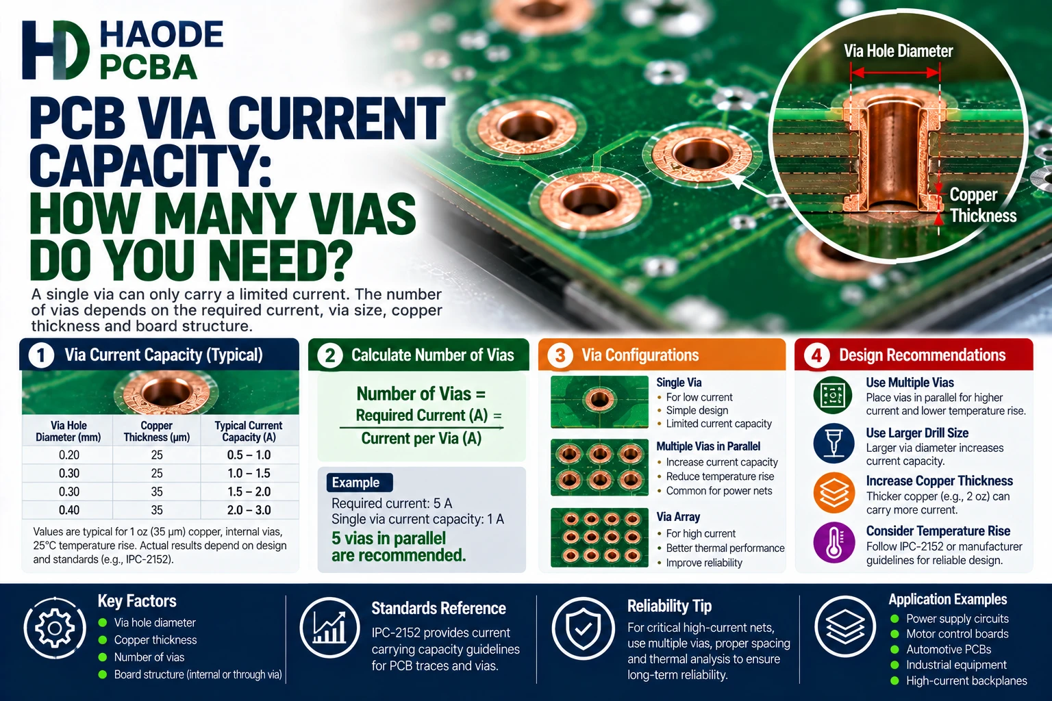
PCB via current capacity cannot be defined by one universal “amps per via” value. It depends on the finished copper cross-section inside the hole, via length, copper resistivity, permitted temperature rise, surrounding planes, current duration, and how evenly parallel vias share current.
A useful design process has two parts:
- Calculate via resistance, voltage drop, and power loss.
- Verify the temperature rise under the actual board and operating conditions.
The first part uses geometry and electrical formulas. The second part requires thermal analysis or physical testing. Therefore, a calculated resistance does not by itself establish a safe current rating.
What Determines PCB Via Current Capacity?
Current flows vertically through the copper barrel of a plated via. Consequently, the barrel’s minimum copper cross-section becomes the first electrical constraint.
The main inputs are:
- Finished-hole diameter
- Minimum hole-wall copper thickness
- Board thickness
- Via type
- Copper resistivity
- Continuous or pulsed current
- Permitted voltage drop
- Permitted temperature rise
- Top and bottom copper area
- Internal plane connections
- Number and spacing of parallel vias
- Ambient temperature
- Airflow
- Nearby heat sources
- Thermal cycling requirements
A small via in a thick board has a longer and narrower current path. In contrast, a larger hole with thicker barrel copper provides lower resistance.
However, geometry alone does not describe heat removal. A via connected to large copper planes may run cooler than an identical via connected through narrow thermal-relief spokes.
How To Calculate PCB Via Resistance
Treat the plated barrel as a short cylindrical conductor.
The approximate copper cross-sectional area is:
A ≈ π × D × t
Where:
- A = copper cross-sectional area
- D = finished internal hole diameter
- t = minimum barrel copper thickness
For greater precision, use the annular-area formula:
A = π ÷ 4 × [(D + 2t)² − D²]
Next, calculate resistance:
R = ρ × L ÷ A
Where:
- R = via resistance
- ρ = copper resistivity
- L = via length or board thickness
- A = barrel copper cross-sectional area
NIST lists the resistivity of standard annealed copper at 20°C as 0.017241 Ω·mm²/m, equivalent to 1.7241 × 10⁻⁸ Ω·m. However, actual plated copper, temperature, thickness variation, and measurement uncertainty can change the finished resistance.
Therefore, use the formula as a design estimate and apply the supplier’s minimum finished hole copper rather than nominal plating targets.
PCB Via Current Capacity Calculation Example
Assume a through via with the following dimensions:
| Input | Example Value |
|---|---|
| Finished-Hole Diameter | 0.30 mm |
| Minimum Barrel Copper | 0.025 mm |
| Finished Board Thickness | 1.60 mm |
| Estimated Copper Resistivity | 0.017241 Ω·mm²/m |
First, estimate the copper cross-sectional area:
A ≈ π × 0.30 mm × 0.025 mm
A ≈ 0.0236 mm²
Next, calculate resistance:
R = 0.017241 × 0.0016 ÷ 0.0236
R ≈ 0.00117 Ω
Therefore, the estimated via resistance is approximately:
1.17 mΩ
At 2 A:
Voltage Drop = I × R
Voltage Drop = 2 × 0.00117 = 2.34 mV
The electrical power converted into heat is:
Power = I² × R
Power = 2² × 0.00117 = 0.00468 W
Therefore, the via produces approximately 4.68 mW of resistive loss at 2 A under the assumed conditions.
This calculation does not mean that the via has a confirmed 2 A current rating. Instead, it gives the designer a resistance and heat-generation estimate that must be evaluated within the actual thermal environment.
Why Resistance Does Not Equal Safe Current
A via does not fail simply because it reaches a particular current value. Instead, current creates heat, and that heat raises the temperature of the barrel and surrounding materials.
The final temperature depends on both heat generation and heat removal:
Temperature Rise = Heat Generated − Heat Removed By The PCB And Environment
Relevant thermal paths include:
- Copper planes
- Surface traces
- Internal planes
- Component pads
- Nearby vias
- Laminate
- Air
- Chassis
- Heat sinks
- Thermal interface materials
Consequently, two vias with identical dimensions can reach different temperatures at the same current.
For example, a via connected directly to large internal power planes may spread heat effectively. Another via connected through narrow neckdowns may create local heating at its entry and exit points.
Therefore, PCB via current capacity must include the complete current path, not only the vertical barrel.
What IPC-2152 Does And Does Not Prove
IPC-2152 defines current-carrying capacity as the maximum continuous current a conductor can carry without unacceptable electrical or mechanical degradation. It also treats conductor size and acceptable temperature rise as connected design variables.
However, designers should understand two important boundaries.
First, IPC-2152 provides general printed-board conductor guidance. A third-party calculator that labels its result “IPC-2152 via current” may still apply additional assumptions or extrapolate conductor data to a cylindrical barrel.
Second, IPC’s current revision table marks IPC-2152 as “No Longer Maintained.” Therefore, engineers may still use its thermal principles and historical data, but they should not describe it as a newly maintained universal via-rating standard.
For critical designs, document the calculation method, assumptions, temperature limit, and verification test rather than citing only “IPC-2152 compliant.”
How Board Thickness Affects PCB Via Current Capacity
A thicker board creates a longer via barrel.
Because resistance increases with conductor length:
Thicker PCB → Longer Barrel → Higher Resistance → More Voltage Drop And Heat
Consider the same 0.30 mm finished via with 0.025 mm barrel copper:
| Board Thickness | Approximate Resistance | Loss At 2 A |
|---|---|---|
| 0.80 mm | 0.59 mΩ | 2.36 mW |
| 1.60 mm | 1.17 mΩ | 4.68 mW |
| 2.40 mm | 1.76 mΩ | 7.04 mW |
| 3.20 mm | 2.34 mΩ | 9.36 mW |
These results assume identical copper geometry and resistivity. In production, however, deep holes may also receive less copper at their centers.
Therefore, board thickness affects both calculated resistance and plating difficulty. The PCB aspect ratio should be reviewed together with current-carrying requirements.
Why Finished Hole Size Matters
A larger barrel circumference provides more copper cross-sectional area when plating thickness remains constant.
Therefore:
Larger Hole Diameter → More Barrel Copper Area → Lower Electrical Resistance
However, designers must distinguish:
- Drill-tool diameter
- Drilled-hole diameter
- Finished-hole diameter
- Minimum finished-hole diameter
- Maximum finished-hole diameter
Plating reduces the open hole diameter while adding conductive copper around the barrel.
The PCB drill size versus finished hole size should therefore guide both the resistance calculation and component-fit requirements.
Do not calculate current capacity from the drill-tool diameter if the formula assumes the finished internal barrel diameter.
How Hole Copper Thickness Changes Via Current Capacity
Barrel copper thickness directly changes conductive cross-sectional area.
For the same 0.30 mm finished hole and 1.60 mm board:
| Barrel Copper Thickness | Approximate Barrel Area | Approximate Resistance |
|---|---|---|
| 0.015 mm | 0.0141 mm² | 1.96 mΩ |
| 0.020 mm | 0.0188 mm² | 1.47 mΩ |
| 0.025 mm | 0.0236 mm² | 1.17 mΩ |
| 0.035 mm | 0.0330 mm² | 0.84 mΩ |
These values use the thin-wall approximation and represent electrical estimates.
The designer should use minimum finished hole copper, not an average or nominal surface-plating value. High aspect ratio holes may contain less copper at the barrel center than near the hole entrances.
Moreover, local PCB plating voids reduce the effective current path even when the average copper thickness appears acceptable.
How Many Parallel Vias Do You Need?
For identical resistances with perfectly equal current sharing:
Total Resistance = Single-Via Resistance ÷ Number Of Vias
If one via measures 1.17 mΩ, four ideal parallel vias produce:
1.17 mΩ ÷ 4 = 0.293 mΩ
If the total current equals 8 A and divides evenly, each via carries 2 A.
However, real layouts rarely divide current perfectly.
Current sharing depends on:
- Via placement
- Distance from the source pad
- Trace geometry
- Plane neckdowns
- Copper thickness
- Via resistance variation
- Thermal gradients
- Connector pin position
- High-frequency inductance
- Switching-loop geometry
The via closest to the current source may carry more current than a distant via. Therefore, designers should not multiply a single-via rating by via count without reviewing the surrounding copper.
Practical Via-Array Workflow
Use the following process:
- Define maximum continuous and pulsed current.
- Calculate the resistance of one via from minimum copper dimensions.
- Select a preliminary number of parallel vias.
- Calculate ideal array resistance and total power loss.
- Review current entry and exit geometry.
- Add margin for unequal sharing and manufacturing variation.
- Simulate or measure temperature rise.
- Confirm voltage drop under maximum current.
- Inspect production hole copper.
- Test the assembly under worst-case ambient conditions.
This workflow produces a defendable design decision. In contrast, a fixed “amps per via” table hides most of the relevant variables.
Via Placement Matters As Much As Via Count
A compact, symmetrical via array normally shares current better than a long row fed from one side.
For example, assume six vias connect a power-device pad to an internal plane. If the trace reaches the first via before the others, the nearest hole may carry a disproportionate part of the current.
To improve sharing:
- Place vias symmetrically around the current source.
- Use wide copper between the source and every via.
- Avoid narrow neckdowns.
- Connect directly to solid planes where possible.
- Keep similar path lengths.
- Avoid placing all vias on only one side of a power pad.
- Review current density at pad corners.
- Use enough copper between adjacent holes.
Adding more vias behind a narrow trace does not increase the capacity of that narrow trace. The smallest copper section still limits the path.
Continuous Current Versus Pulsed Current
A short pulse may not raise the via to the same temperature as continuous current because the copper and surrounding PCB absorb heat over time.
However, pulse evaluation requires:
- Peak current
- Pulse duration
- Duty cycle
- Repetition frequency
- RMS current
- Initial board temperature
- Thermal time constant
- Electrical inductance
- Allowed voltage transient
For repetitive current pulses, calculate RMS heating:
Iᵣₘₛ = √[(I₁²t₁ + I₂²t₂ + …) ÷ Total Period]
Nevertheless, RMS current alone may not capture peak voltage drop, current crowding, fusing risk, or switching inductance.
Therefore, power converters, motor drives, battery systems, and pulsed loads require both electrical and thermal verification.
DC Current Versus High-Frequency Current
At DC and low frequency, barrel resistance often dominates the via’s electrical loss.
At higher frequencies, designers must also consider:
- Via inductance
- Return-path geometry
- Current-loop area
- Skin and proximity effects
- Plane transitions
- Switching edge rate
- Simultaneous switching noise
- Parallel-via spacing
Multiple ground-return vias may improve high-frequency performance even when one via could carry the DC current.
Therefore, a via count selected only from DC resistance may remain inadequate for fast switching or high-speed signals.
Power Vias And Thermal Vias Are Not The Same
A power via transfers electrical current between copper layers.
A thermal via transfers heat away from a component pad, exposed pad, copper coin, or hot region.
The same physical via can carry both electrical current and heat. However, the design objective changes.
Power Via Priorities
For power transfer, review:
- Barrel resistance
- Voltage drop
- Current sharing
- Hole copper
- Entry and exit geometry
- Reliability under electrical load
Thermal Via Priorities
For heat transfer, review:
- Total copper-barrel area
- Via count
- Via pitch
- Via length
- Connection to spreading planes
- Fill material
- Solder wicking
- Component-pad layout
- Heat-sink path
A large number of small thermal vias may spread heat effectively across a component pad. However, the same array may not share high electrical current evenly if the copper feed geometry remains unbalanced.
Does Via Filling Increase Current Capacity?
The answer depends on the fill material.
Nonconductive Resin Fill
Nonconductive resin does not create an additional electrical path through the hole.
Therefore, calculate electrical current from the copper barrel, not from the filled center.
Resin filling may improve surface planarity and enable via-in-pad assembly, but it does not turn the hole into a solid copper conductor.
Conductive Epoxy Fill
Conductive epoxy may provide some electrical and thermal conduction. However, its resistivity usually differs substantially from electrodeposited copper.
Do not count the fill as copper unless the supplier provides qualified material properties, process data, and finished-structure verification.
Copper-Filled Microvias
A copper-filled microvia contains more conductive metal than a hollow plated barrel. Nevertheless, current still depends on microvia geometry, target-land contact, interface integrity, and stacked construction.
Our microvia copper filling article explains fill quality, dimples, voids, cap plating, and target interfaces.
How Manufacturing Defects Reduce PCB Via Current Capacity
The calculation assumes a continuous copper barrel with uniform thickness. Production defects violate that assumption.
Potential problems include:
- Thin center-barrel copper
- Plating voids
- Rough or nodular copper
- Incomplete electroless copper
- Inner-layer separation
- Resin smear
- Drill damage
- Barrel cracks
- Target-land separation
- Microvia fill voids
A via can pass initial electrical testing yet contain limited thermal or mechanical margin.
Furthermore, repeated heating changes barrel dimensions relative to the surrounding laminate. If the copper lacks sufficient ductility, cracks may form around high-stress regions.
The PCB copper ductility article explains why elongation and tensile behavior matter in addition to copper thickness.
Likewise, PCB barrel cracks can increase resistance, create intermittent faults, or eventually open the current path.
How To Verify PCB Via Current Capacity
Use several forms of evidence because no single test answers every question.
| Verification Method | What It Shows | Important Limitation |
|---|---|---|
| Resistance Calculation | Expected voltage drop and loss | Does not establish actual temperature |
| DC Resistance Measurement | Finished electrical resistance | May not locate thin or defective copper |
| Thermal Imaging | Surface-temperature distribution | May not reveal the hottest internal interface |
| Thermocouple Measurement | Local temperature over time | Placement can affect the result |
| Microsection | Barrel thickness and structural quality | Destructive and sample-based |
| Current Cycling | Response to repeated electrical heating | Requires defined current and cycle conditions |
| Thermal Cycling | Mechanical reliability under expansion | Does not reproduce every powered condition |
| Functional Load Test | System behavior under actual load | May not isolate via temperature |
| Four-Wire Measurement | Small resistance changes | Needs suitable test access and equipment |
Measure The Worst-Case Board
Testing should represent:
- Maximum current
- Maximum ambient temperature
- Minimum airflow
- Highest component dissipation
- Minimum production hole copper
- Maximum board thickness
- Enclosure conditions
- Worst supply voltage
- Longest operating duration
A room-temperature bench test in open air may not represent a sealed product in summer operation.
Inspect Minimum Hole Copper
A PCB microsection should examine the barrel center as well as the top and bottom regions.
Request:
- Minimum copper thickness
- Measurement locations
- Hole diameter
- Board thickness
- Aspect ratio
- Panel position
- Sample quantity
- Magnification
- Raw microsection images
- Applicable acceptance criteria
Average copper thickness alone can hide a thin center region.
How Board Temperature Changes Resistance
Copper resistance increases as temperature rises.
Therefore, a via that measures 1.17 mΩ near room temperature will have higher resistance when hot. Higher resistance creates additional I²R loss, which can increase temperature further.
This does not automatically create thermal runaway because heat dissipation also increases with temperature difference. Nevertheless, it shows why a room-temperature resistance calculation cannot replace thermal validation.
Designers should use the expected operating temperature or temperature-dependent material data when voltage drop becomes critical.
PCB Via Current Capacity DFM Checklist
Before releasing a high-current design, verify:
- Is the maximum continuous current defined?
- Are pulse magnitude, duration, and duty cycle defined?
- Is the permitted voltage drop defined?
- Is the permitted temperature rise defined?
- Does the calculation use minimum barrel copper?
- Does it use maximum board thickness?
- Does it use the correct finished barrel diameter?
- Has the via aspect ratio been checked?
- Can the manufacturer plate the barrel center consistently?
- Are parallel vias positioned symmetrically?
- Do top and bottom traces support the same current?
- Are internal planes free from narrow neckdowns?
- Do thermal-relief spokes limit the path?
- Does the design include margin for uneven sharing?
- Are high-frequency return paths adequate?
- Is the fill material conductive or nonconductive?
- Are plating voids and barrel cracks controlled?
- Will the design experience repeated power cycling?
- Does the inspection plan include representative microsections?
- Will the assembly undergo a worst-case load test?
- Has the manufacturer completed a PCB DFM review?
What Buyers Should Include In The RFQ
For high-current vias, provide:
- Maximum continuous current
- Peak current
- Pulse duration
- Duty cycle
- Allowed voltage drop
- Allowed temperature rise
- Ambient-temperature range
- Cooling conditions
- Finished board thickness
- Via drill and finished-hole dimensions
- Via count and array geometry
- Required minimum hole copper
- Copper weight by layer
- Plane and trace geometry
- Fill requirement
- Applicable IPC class and revision
- Microsection requirements
- Current-load test requirements
- Thermal-test conditions
- Prototype and production quantities
Additionally, ask the supplier to confirm:
- Minimum finished barrel copper
- Maximum supported aspect ratio
- Plating distribution control
- Sampling plan
- Microsection locations
- Thermal-stress requirements
- Any special plating process
- Production panel limitations
- Expected hole-size tolerance
Include this information when requesting a PCB assembly quote so the supplier can assess fabrication and powered-assembly risk together.
Frequently Asked Questions About PCB Via Current Capacity
How Many Amps Can One PCB Via Carry?
There is no universal value. Calculate the barrel resistance and power loss from actual geometry, then verify the temperature rise under the intended operating conditions.
Can A 0.3 mm Via Carry 2 A?
It may, depending on barrel copper, board thickness, surrounding copper, ambient temperature, airflow, current duration, and permitted temperature rise.
The diameter alone cannot answer the question.
Do Four Vias Carry Four Times The Current?
Only if the current divides appropriately and the surrounding copper supports the total load. Real arrays often share current unevenly.
Therefore, include layout margin and verify the finished design.
Does A Larger Pad Increase Via Current Capacity?
A larger pad can spread heat and reduce current crowding around the via entrance. However, it does not increase the barrel copper cross-section unless the hole or plating thickness also changes.
Does Thicker Surface Copper Increase Via Current Capacity?
Thicker traces and planes can reduce horizontal resistance and improve heat spreading. Nevertheless, surface copper thickness does not prove minimum copper at the barrel center.
Does Resin-Filled Via-In-Pad Carry More Current?
Nonconductive resin does not add an electrical current path. Calculate current through the plated copper unless the fill system provides qualified conductive properties.
Are Copper-Filled Microvias Better For High Current?
Copper filling can reduce electrical and thermal resistance. However, target contact, interface integrity, stacking, via size, and manufacturing quality still control reliability.
Can Electrical Testing Confirm Via Current Capacity?
No. A continuity test confirms that the connection conducts at the test condition. It does not prove acceptable temperature rise, power-cycling life, or minimum structural margin.
Should High-Current Vias Use Thermal Relief?
Thermal relief may help soldering, but narrow spokes can restrict electrical current and heat flow.
Review the spoke count, width, copper thickness, soldering process, and current requirement together.
What Is The Best Way To Increase Via Current Capacity?
Use a combination of:
- More parallel vias
- Larger finished holes
- Thicker hole copper
- Shorter via length
- Wider surface copper
- Direct plane connections
- Balanced via placement
- Better heat spreading
Then verify temperature under maximum operating load.
Final Recommendations For PCB Via Current Capacity
Reliable PCB via current capacity requires more than a lookup table.
Use this engineering sequence:
- Define the current waveform and temperature limit.
- Calculate barrel area from minimum finished copper.
- Calculate via resistance, voltage drop, and I²R loss.
- Select a preliminary parallel-via array.
- Review current sharing and surrounding copper.
- Check aspect ratio and plating capability.
- Inspect minimum hole copper.
- Test voltage drop and temperature at maximum load.
- Repeat the test under worst-case product conditions.
- Document the assumptions and acceptance limits.
The key relationship is:
Barrel Geometry → Via Resistance → I²R Loss → Heat Distribution → Temperature Rise → Reliability
A calculation can estimate electrical loss. However, only a defined thermal environment and verification test can support the final current decision.