
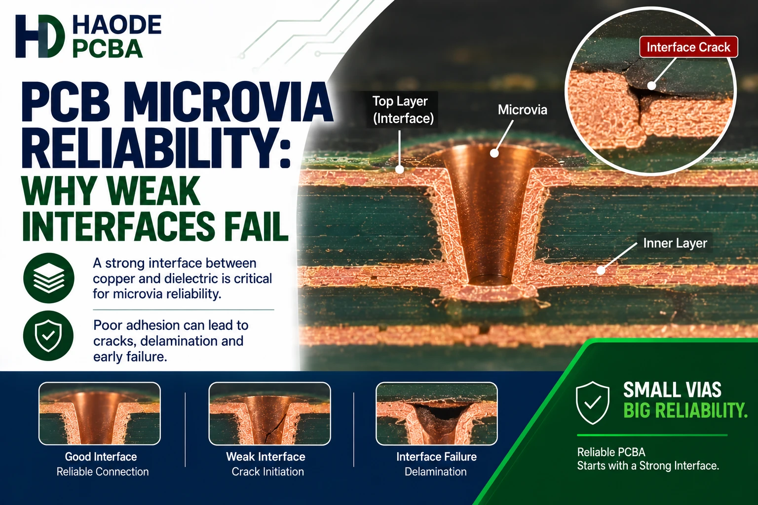
PCB microvia reliability depends on the integrity of the copper connection between a laser-drilled microvia and its target pad. A microvia can pass bare-board electrical testing and appear acceptable in a room-temperature microsection yet separate during multiple lead-free reflow cycles.
The highest risk does not come from microvia diameter alone. Instead, buyers must evaluate target-pad preparation, copper coverage, via filling, stacked interfaces, sequential lamination, material expansion, assembly temperature, and performance-based testing.
Therefore, a dimensional inspection cannot provide complete evidence of microvia reliability.
What Is a PCB Microvia?
A microvia is a small blind or buried connection that usually joins adjacent copper layers in an HDI structure. Manufacturers commonly form microvias with laser drilling rather than mechanical drilling.
A typical microvia contains:
- An opening on the upper copper layer
- A dielectric sidewall
- Copper plating or copper fill
- A target pad on the lower layer
- A copper interface connecting the via to the target
NASA’s overview of PCB risks and supplier capability describes microvias as blind or buried vias with small diameters and capture pads. However, the project should use the definition in its specified IPC document and revision.
Microvias allow designers to:
- Escape fine-pitch BGA pads
- Reduce via-pad dimensions
- Increase routing density
- Shorten signal paths
- Connect sequential build-up layers
- Use via-in-pad structures
- Reduce mechanically drilled through-hole demand
However, every additional build-up layer, lamination cycle, and microvia interface adds manufacturing variables that require control.
The approved multilayer PCB stackup should show where each microvia starts, where it terminates, and how the sequential lamination structure connects.
Why Can PCB Microvia Reliability Fail After Reflow?
Laminate, resin, copper foil, and plated copper respond differently to heat.
During lead-free reflow, the PCB expands. When it cools, the materials contract. This movement places tensile and shear stress on the microvia and its target-pad interface.
If the interface is weak, one or more reflow cycles may initiate or enlarge a separation.
The failure can remain hidden because:
- The separated surfaces may contact each other after cooling.
- The crack may affect only part of the interface.
- Room-temperature resistance may remain within the tester’s limit.
- The inspected microsection may sample a different microvia.
- Optical inspection may not resolve the weak boundary.
- Standard X-ray may not show a thin horizontal separation.
As a result, a board can pass fabrication inspection and fail later during:
- SMT reflow
- Double-sided assembly
- Rework
- In-circuit testing
- Environmental screening
- Product operation
The Global Electronics Association’s microvia reliability warning notes that some microvia failures appeared only after fabrication acceptance, reflow, box-level testing, or field use.
Where Do Microvias Fail?
A microvia can fail at several locations.
| Failure Location | Possible Mechanism | Evidence Needed |
|---|---|---|
| Microvia-To-Target Interface | Weak copper bond or contaminated target pad | Targeted cross-section and interface analysis |
| Bottom Corner Of Microvia | Local stress concentration or thin copper | Microsection through true via center |
| Copper Fill | Internal void, seam, or inclusion | X-ray and destructive section |
| Interface Between Stacked Vias | Weak plated interface or poor planarization | Sections through the complete stack |
| Capture Pad | Pad cracking or local copper weakness | Metallographic analysis |
| Dielectric Interface | Delamination or resin damage | Cross-section and material review |
| Surface Cap Copper | Insufficient cap or planarization damage | Surface and cross-sectional measurement |
A horizontal separation at the target pad differs from a crack through the plated sidewall.
Likewise, a fill void differs from an adhesion defect. Consequently, the failure report should identify the exact physical interface instead of using “microvia crack” as the final root cause.
Some failures resemble PCB interconnect defects because both involve separation between copper structures. Nevertheless, microvia geometry, laser processing, filling, and sequential lamination create different process risks.
What Is a Weak Microvia Interface?
A weak microvia interface occurs when the plated or filled copper does not form a sufficiently reliable bond with the underlying target pad.
The interface may remain electrically conductive at room temperature. However, thermal strain can progressively separate it.
Possible contributors include:
- Residue on the target pad
- Oxidized or contaminated copper
- Incomplete laser-debris removal
- Excessive target-pad damage
- Poor microetch control
- Weak electroless copper coverage
- Inadequate copper-to-copper adhesion
- Plating additives or residues
- Insufficient rinsing
- Voids near the interface
- Excessive thermal stress
- Multiple stacked interfaces
IPC-WP-023 focuses on the hidden reliability threat associated with weak microvia interfaces and stacked structures. The related IPC white paper description emphasizes performance-based acceptance rather than reliance on traditional visual inspection alone.
However, finding a separation does not automatically identify which chemical or mechanical step caused it. The manufacturer must compare the defect with process records and control samples.
How Does Target-Pad Preparation Affect Reliability?
Laser drilling removes dielectric material and exposes the copper target pad. The resulting surface must support a strong metallurgical connection.
Target-pad preparation may involve:
- Laser-residue removal
- Plasma treatment
- Chemical cleaning
- Microetching
- Conditioning
- Rinsing
- Activation
- Primary metallization
If residue remains, subsequent copper can cover it without forming a reliable bond to the target pad.
Conversely, excessive treatment can:
- Roughen the target excessively
- Reduce copper thickness
- Damage the pad
- Change microvia geometry
- Leave chemical residues
- Create inconsistent surface conditions
The following PCB electroless copper process must provide continuous initial coverage. However, complete coverage does not automatically prove strong target-pad adhesion.
Therefore, the supplier should qualify laser drilling, cleaning, activation, and copper deposition as one connected process.
Stacked vs. Staggered Microvia Reliability
1.Stacked and staggered structures solve different routing problems.
| Structure | Construction | Main Advantage | Main Reliability Consideration |
|---|---|---|---|
| Single-Level Microvia | One Via Connects Adjacent Layers | Simple HDI Interconnection | One Primary Microvia Interface |
| Staggered Microvias | Vias On Successive Layers Are Offset | Avoids Direct Vertical Stacking | Uses More Routing And Pad Area |
| Two-Level Stacked Microvias | One Microvia Sits Above Another | Saves Space And Supports Dense Routing | Requires Reliable Fill, Planarization, And Stacked Interface |
| Multi-Level Stacked Microvias | Several Microvias Align Vertically | Maximum Vertical Density | Adds More Dependent Interfaces And Sequential Processes |
Stacked microvias are not automatically defective. Manufacturers successfully produce qualified stacked structures for many applications.
However, every aligned level depends on:
- Complete copper fill
- Suitable cap copper
- Controlled planarization
- Clean copper interfaces
- Accurate registration
- Stable sequential lamination
- Qualified thermal performance
Staggering microvias can reduce the number of directly aligned interfaces. Nevertheless, a staggered design can still fail if the individual vias contain weak target-pad bonds, voids, or insufficient copper.
Therefore, design teams should choose the least complex structure that meets routing and component-density requirements.
Does Microvia Aspect Ratio Matter?
Microvia aspect ratio usually compares the dielectric depth with the laser-drilled opening or finished diameter.
A deeper, narrower microvia can make the following operations more difficult:
- Laser-debris removal
- Target-pad cleaning
- Wetting
- Catalyst coverage
- Copper deposition
- Via filling
- Void prevention
- Inspection
A lower aspect ratio generally provides more process margin. However, no single ratio guarantees reliability.
Two vias with the same nominal ratio may behave differently because of:
- Different dielectric materials
- Different laser profiles
- Different target-pad conditions
- Different plating chemistry
- Different opening and bottom diameters
- Different filling processes
- Different lamination histories
The design should therefore use a manufacturer-approved PCB aspect ratio for the exact HDI construction.
The supplier should review actual dielectric thickness after lamination rather than calculating the ratio only from nominal prepreg values.
How Do Copper-Fill Voids Affect Microvias?
Copper filling should produce a controlled structure without harmful internal discontinuities.
Potential fill conditions include:
- Complete solid fill
- Centerline seam
- Small isolated void
- Large internal void
- Bottom void
- Incomplete fill
- Surface dimple
- Overplated cap
- Trapped contamination
A void changes the load path through the copper. It can also create a local stress concentration or reduce the effective conductive area.
However, not every visible microvia void has the same reliability effect. Evaluation should consider:
- Void size
- Void location
- Number of voids
- Distance from the target interface
- Remaining copper
- Via diameter
- Stack level
- Product requirement
- Applicable acceptance criteria
A general PCB plating void article may explain continuity and hole-wall defects, but filled microvias require geometry-specific evaluation.
X-ray can help identify larger fill voids. Nevertheless, it may not reveal a thin target-pad separation or identify whether the copper bond will survive reflow.
Why Is Planarization Important for Stacked Microvias?
Before the manufacturer places another microvia above a filled via, the underlying surface must support the next build-up layer.
Planarization controls:
- Surface flatness
- Remaining cap copper
- Local dish or protrusion
- Copper cleanliness
- Lamination contact
- Laser focus
- Registration
- Next-level target geometry
Excessive grinding can reduce cap copper or expose a weak area. Insufficient planarization can create uneven lamination or distort the next laser-drilled structure.
Therefore, stacked microvia reliability depends on more than filling the lower via. It also depends on the surface that receives the next dielectric and via level.
The fabrication drawing should define critical cap, fill, and planarization requirements where the applicable standard or product design requires them.
Can Room-Temperature Electrical Testing Find Microvia Failures?
Room-temperature electrical testing detects opens and shorts present during the test.
It may not detect a latent microvia separation when:
- The interface reconnects after cooling
- Resistance change remains below the tester limit
- Mechanical contact maintains temporary continuity
- The crack develops only at high temperature
- Repeated cycling has not yet enlarged the defect
Therefore, a bare-board electrical test is necessary but insufficient for high-risk microvia qualification.
A stronger strategy uses a daisy-chain coupon and continuously monitors resistance during:
- Reflow simulation
- Thermal cycling
- IST
- Another specified performance test
The key question is not only whether the circuit works after cooling. Instead, the test should determine whether resistance changes while thermal stress acts on the interface.
Why Can Microsection Inspection Miss a Weak Interface?
Microsectioning remains valuable, but it examines only selected physical locations.
A section can miss the failure because:
- It samples an unaffected microvia.
- It does not pass through the true via center.
- The crack lies outside the section plane.
- Polishing smears copper across a separation.
- The interface closes at room temperature.
- Magnification or lighting is insufficient.
- The defect develops only after additional reflow.
- The coupon does not represent the critical structure.
IPC’s warning states that traditional thermally stressed microsections and light microscopy alone may not reliably detect certain microvia-to-target plating failures.
Therefore, a PCB microsection should support performance testing rather than replace it.
When a test coupon fails electrically, the laboratory should first localize the damaged via and then section that region.
Which Tests Provide the Strongest Evidence?
No single test proves every aspect of microvia reliability.
| Evidence | What It Can Show | What It Cannot Prove Alone |
|---|---|---|
| Room-Temperature Electrical Test | Current Continuity At Test Time | High-Temperature Interface Stability |
| X-Ray | Fill Voids, Alignment, And Density Differences | Thin Copper-To-Copper Separation |
| As-Fabricated Microsection | Geometry, Fill, And Sampled Interfaces | Every Via Or Future Thermal Performance |
| Reflow Continuity Test | Resistance Behavior During Assembly-Like Heating | Long-Term Field Cycling |
| IST | Cycles To A Defined Resistance Threshold | Direct Product Service Life |
| Thermal Shock Or Cycling | Response To Repeated Temperature Change | Exact Failure Interface Without Analysis |
| SEM Or Elemental Analysis | Sampled Interface Morphology Or Residue | Full-Lot Reliability |
| Destructive Failure Analysis | Confirmed Physical Failure Location | Defect Rate Without Sampling Data |
PCB IST testing can compare representative microvia structures through controlled thermal cycling. However, its value depends on coupon design, preconditioning, threshold, and failure analysis.
Likewise, PCB reflow soldering data should show the actual board temperature rather than only the oven setpoint.
How Should a Microvia Coupon Be Designed?
A qualification or acceptance coupon should represent the structures that create the actual risk.
The coupon should consider:
- Microvia diameter
- Dielectric depth
- Target-pad size
- Capture-pad size
- Single, staggered, or stacked construction
- Number of stacked levels
- Filled or conformal plating
- Via pitch
- Layer connections
- Copper weight
- Stackup
- Laminate type
- Sequential lamination count
- Production plating process
- Panel location
A coupon containing easy, single-level microvias cannot validate a product that uses a more complex stacked structure.
Furthermore, the test coupon should travel through the same relevant production processes as the board. A separately manufactured laboratory coupon may not represent actual lamination, laser drilling, plating, or panel distribution.
What Does a Useful Microvia Test Report Include?
A strong report should record:
- PCB part number and revision
- Lot and panel identification
- Coupon design and revision
- Panel location
- Approved stackup
- Laminate manufacturer and grade
- Sequential lamination structure
- Microvia start and stop layers
- Laser-drilled diameter
- Dielectric depth
- Target and capture-pad dimensions
- Stacked or staggered configuration
- Copper-fill method
- Preconditioning profile
- Number of reflow cycles
- Peak coupon temperature
- Resistance measurement method
- Failure threshold
- Individual coupon results
- Raw resistance curves
- Failure-localization method
- Microsection images
- Confirmed failure interface
The report should not provide only “pass” or “fail.”
For example, a coupon that fails during the second simulated reflow presents a different risk from one that remains stable through preconditioning and fails much later during cycling.
How Should Buyers Specify PCB Microvia Reliability?
A practical procurement note could state:
Microvia structures shall reproduce the approved stackup, sequential lamination sequence, via dimensions, target pads, copper-fill process, and stacked or staggered configuration. Representative production-panel coupons shall receive the specified assembly preconditioning and resistance-monitored performance test. Report individual coupon data and perform targeted physical analysis on any coupon that reaches the failure threshold.
The buyer should add project-specific:
- Applicable IPC document and revision
- Required coupon quantity
- Panel positions
- Preconditioning cycles
- Peak temperature
- Resistance threshold
- Required test cycles
- Acceptance criteria
- Retest rules
- Data-retention requirements
Avoid relying on a note such as “microvias per IPC.” It does not identify the construction, test condition, or required evidence.
PCB Microvia Reliability DFM Checklist
Before releasing an HDI design, confirm:
- Does the product require stacked microvias?
- Can any levels use a staggered structure?
- How many sequential lamination cycles are required?
- What are the actual dielectric depths?
- Are laser-drilled diameters manufacturer-approved?
- Does each microvia have adequate target and capture pads?
- Is the fill and planarization process qualified?
- Does the test coupon reproduce the complete stack?
- Are coupon panel locations defined?
- How many assembly reflow cycles will occur?
- Will resistance be monitored during thermal testing?
- Is the failure threshold specified?
- Must failed coupons receive targeted sectioning?
- Are material substitutions prohibited without approval?
- Does the manufacturer have production data for the same structure?
These questions should form part of the PCB DFM checklist before routing and stackup approval become fixed.
Final PCB Microvia Reliability Recommendation
PCB microvia reliability requires more evidence than dimensional inspection and room-temperature continuity.
A reliable microvia process connects five elements:
Clean Target Pad → Continuous Copper Interface → Controlled Fill And Planarization → Representative Thermal Testing → Confirmed Failure Analysis
For lower risk:
- Use the simplest microvia architecture that meets routing needs.
- Avoid unnecessary stacked levels.
- Confirm actual dielectric depth and via geometry.
- Qualify the exact laminate and sequential lamination process.
- Monitor electrical resistance during reflow or thermal cycling.
- Use coupons from representative panel locations.
- Analyze every unexplained early failure.
When a microvia fails, a structured PCBA failure analysis should identify the physical interface before the supplier changes laser, cleaning, plating, filling, or lamination parameters.
The most important conclusion is:
A microvia that passes at room temperature is not proven reliable until its critical interfaces survive the thermal conditions that represent manufacturing and use.