A Well-Designed Circuit Board Pattern Turns An Electrical Idea Into A Manufacturable PCB With Stable Signals, Reliable Power Delivery, And Fewer Production Risks.
What Is A Circuit Board Pattern?
A Circuit Board Pattern Is The Planned Arrangement Of Traces, Pads, Vias, Copper Areas, And Component Connection Points On A Printed Circuit Board.
In Design Software, The Pattern Appears As Layout Geometry. After Fabrication, The Approved Pattern Becomes The Conductive Copper Structure That Carries Power And Signals.
Why Does A Circuit Board Pattern Matter?
A PCB Does Not Work Only Because Components Are Selected Correctly. Those Components Must Also Be Connected Through A Controlled Electrical Path.
A Good PCB Trace Pattern Helps Reduce Signal Loss, Manage Current Flow, Improve Thermal Performance, Limit Noise, And Support Reliable PCB Manufacturing.
Is A Circuit Board Pattern The Same As A PCB Layout?
A Circuit Board Pattern Usually Refers To The Copper Connection Geometry On A Board. A PCB Layout Is Broader And Includes Component Placement, Board Shape, Keep-Out Areas, Mechanical Holes, Layer Stack-Up, Labels, And Routing.
For Manufacturing, Both Must Work Together. Correct Traces Cannot Fix Incorrect Component Placement Or An Incompatible Board Outline.
Circuit Board Pattern Vs. Schematic Vs. Footprint Vs. Gerber
These Terms Describe Different Stages Of PCB Development. Confusing Them Can Lead To Design Errors Or Incorrect Manufacturing Files.
| Term | What It Represents | Why It Matters |
|---|---|---|
| Schematic | Logical Electrical Connections | Defines What Must Connect |
| Footprint | Physical Pad Layout For A Component | Ensures Correct Assembly Fit |
| Circuit Board Pattern | Traces, Pads, Vias, Planes, And Copper Routing | Controls Electrical Pathways |
| PCB Layout | Full Physical Board Design | Coordinates Placement And Routing |
| Gerber Files | Manufacturing Output Data | Allows The Factory To Produce The PCB |
What Does A Circuit Board Pattern Include?
A Complete Printed Circuit Board Pattern Uses Several Copper And Mechanical Elements To Form A Working Circuit.
| Pattern Element | Function | Design Focus |
| Traces | Carry Power Or Signals | Width, Length, Spacing, Current |
| Pads | Connect Component Pins To Copper | Size, Shape, Solderability |
| Vias | Connect Copper Between Layers | Drill Size, Placement, Reliability |
| Copper Pours | Fill Larger Copper Areas | Grounding, Heat, Current Flow |
| Power Planes | Distribute Supply Voltage | Low Impedance Delivery |
| Ground Planes | Provide Return Paths | Noise And EMI Control |
| Differential Pairs | Carry Balanced High-Speed Signals | Spacing And Impedance |
| Thermal Reliefs | Connect Pads To Large Copper Areas | Soldering And Heat Balance |
How Does A PCB Pattern Carry Signals And Power?
Conductive Traces Act As Electrical Pathways Between Components. Pads Attach Components To The Circuit, While Vias Move Signals Or Power Between Layers.
Power And Ground Areas Support Stable Voltage And Return Current Flow. Their Arrangement Affects Noise, Heat, Signal Integrity, And Long-Term Reliability.
What Makes A Good PCB Pattern Design?
A Good PCB Pattern Design Connects Every Required Net While Respecting Electrical, Mechanical, Thermal, And Manufacturing Limits.
It Should Use Clear Routing Priorities, Stable Reference Planes, Correct Footprints, Suitable Trace Widths, Proper Spacing, And Verified Fabrication Rules.
What Are The Main Circuit Board Pattern Design Guidelines?
1. Confirm Electrical Connectivity First
Every Net In The Schematic Must Reach The Correct Pad, Via, Connector, Or Copper Area On The PCB.
Design Rule Checking Helps Identify Missing Connections, Incorrect Clearances, Shorts, Or Unrouted Nets Before Production.
2. Place Components Before Routing Traces
Component Placement Directly Affects Routing Length, Noise, Heat, Assembly Access, And Board Size.
Place Related Components Close Together. Keep Decoupling Capacitors Near Power Pins And Keep Sensitive Circuits Away From Noisy Switching Areas.
3. Route Critical Signals Before General Signals
High-Speed Interfaces, Clocks, Differential Pairs, RF Lines, And Sensitive Analog Nets Usually Need Priority.
Routing These Signals First Helps Preserve Length Targets, Return Paths, Spacing, And Controlled Impedance Requirements.
4. Design Power And Ground Early
Stable Power Delivery Requires More Than Wide Copper. The Board Also Needs Short Return Paths, Suitable Decoupling, And Correct Ground Structures.
A Solid Ground Plane PCB Design Can Reduce Loop Area, Limit Noise, And Support Cleaner Signal Operation.
5. Match Trace Width To Current And Manufacturing Capability
A Trace That Carries More Current Usually Needs More Copper Width, More Copper Thickness, Or Better Heat Dissipation.
A Trace That Is Too Narrow Can Create Excessive Heating Or Voltage Drop. Final Dimensions Should Be Verified With The PCB Manufacturer.
6. Control Trace Spacing And Clearance
Spacing Affects Manufacturability, Signal Coupling, Voltage Isolation, And Electrical Noise.
Small Spacing Can Support Compact boards, But It May Increase Manufacturing Difficulty And Crosstalk Risk In Sensitive Circuits.
7. Use Vias Carefully
Vias Enable Multilayer Routing, But Each Via Adds Geometry, Manufacturing Requirements, And Electrical Effects.
Avoid Unnecessary Via Transitions On Fast Signals. Use Suitable Via Structures For Power, Thermal Transfer, Or Dense Routing Needs.
8. Include Thermal Management In The Pattern
Heat Can Reduce Component Life And Affect Board Stability.
Copper Pours, Thermal Vias, Heat-Spreading Areas, And Proper Placement Help Manage Temperature Around Regulators, LEDs, Power Devices, And Other Hot Components.
9. Design For Manufacturing Before Ordering
PCB Design For Manufacturability Checks Whether The Board Can Be Built And Assembled Consistently.
Before Fabrication, Confirm Trace Width, Clearance, Hole Size, Annular Ring, Solder Mask, Silkscreen, Copper-To-Edge Distance, Panel Needs, And Assembly Access.
What Is The Difference Between Pattern And Footprint?
A Pattern Controls How Electrical Paths Travel Across The PCB. A Footprint Controls How A Specific Component Physically Mounts To The Board.
| Comparison Point | Circuit Board Pattern | Component Footprint |
| Main Purpose | Routes Power And Signals | Mounts One Component |
| Includes | Traces, Vias, Planes, Copper Areas | Pads, Outline, Pin Numbering |
| Electrical Role | Connects Circuits Across The Board | Connects Component Leads To Pads |
| Mechanical Role | Supports Board-Level Routing | Confirms Physical Fit |
| Common Failure | Noise, Opens, Shorts, Poor Routing | Wrong Pinout, Wrong Size, Misalignment |
| Verification | DRC, Signal Review, Manufacturing Check | Datasheet And Library Verification |
What Types Of Circuit Board Patterns Are Commonly Used?
Single-Sided Circuit Board Pattern
A Single-Sided PCB Pattern Places Conductive Copper Routing On One Side Of The Board.
It Is Suitable For Simple Circuits, Basic Controls, Low-Cost Products, And Designs With Limited Component Density.
Double-Sided Circuit Board Pattern
A Double-Sided PCB Pattern Uses Copper Traces On Both Sides Of The Board And Vias To Connect Between Layers.
It Offers Greater Routing Flexibility Than A Single-Sided Board While Remaining Practical For Many Standard Electronic Products.
Multilayer Circuit Board Pattern
A Multilayer PCB Design Uses Four Or More Conductive Layers Separated By Insulating Materials.
Internal Layers Can Support Signals, Power, Or Ground. This Structure Is Useful For Dense Components, Compact Products, High-Speed Circuits, And More Complex Electronics.
Power Plane Pattern
A Power Plane Pattern Uses Larger Copper Areas To Distribute Supply Voltage Across The PCB.
A Low-Impedance Power Path Helps Reduce Voltage Drop And Supports Stable Operation For Devices With Multiple Active Components.
Ground Plane Pattern
A Ground Plane Pattern Provides A Large Copper Reference Area For Current Return Paths.
Good Grounding Can Reduce Noise, Support Signal Integrity, Improve EMI Performance, And Simplify Routing For Digital Or Mixed-Signal Designs.
Differential Pair Pattern
A Differential Pair Routing Pattern Uses Two Traces That Carry Related Opposite Signals.
This Structure Is Common In USB, Ethernet, HDMI, CAN, LVDS, And Other Interfaces Where Noise Immunity And Signal Timing Matter.
Clock Distribution Pattern
A Clock Pattern Delivers Timing Signals To Processors, Memory Devices, Controllers, Or Communication Circuits.
Clock Routes Need Careful Length, Return Path, Noise, And Coupling Control Because Clock Errors Can Affect The Entire System.
RF Transmission Line Pattern
An RF PCB Pattern Controls The Physical Path Of High-Frequency Signals.
RF Designs Often Need Controlled Impedance, Suitable Grounding, Short Signal Paths, Smooth Routing, And Careful Placement Of Connectors And Matching Components.
How Do Circuit Board Patterns Affect Signal Integrity?
Signal Integrity Describes Whether A Signal Reaches Its Destination With Acceptable Timing, Shape, And Voltage Quality.
A Poor Pattern Can Create Reflections, Crosstalk, Noise, Delay, Or Data Errors. A Better Pattern Controls Geometry, Reference Planes, Spacing, Length, And Via Usage.
When Is Controlled Impedance Needed?
Controlled Impedance Matters When Signal Behavior Depends On Trace Geometry And Layer Structure.
It Is Often Required For High-Speed Digital Interfaces, RF Circuits, Antennas, Differential Pairs, Communication Boards, And Products With Defined Signal Protocols.
Why Does Return Path Matter In PCB Routing?
Every Signal Current Needs A Return Path. The Best Return Path Is Usually Short, Continuous, And Close To The Signal Route.
Routing A Fast Signal Over A Split Plane Or Through A Poor Reference Area Can Increase Noise, EMI, And Signal Instability.
How Can PCB Patterns Reduce EMI And Crosstalk?
PCB Layout And Routing Choices Strongly Affect Electromagnetic Interference And Coupling Between Signals.
| Design Risk | Pattern Improvement |
| Long Noisy Traces | Shorten Routes And Improve Placement |
| Large Current Loops | Keep Signal And Return Paths Close |
| Parallel Sensitive Traces | Increase Spacing Or Change Layers |
| Broken Ground Reference | Use Continuous Ground Paths |
| Uncontrolled Fast Signals | Apply Impedance And Length Control |
| Noisy Power Area | Add Proper Decoupling And Plane Planning |
How Do Circuit Board Patterns Support Power Integrity?
Power Integrity Depends On Stable Voltage Reaching Components Without Excessive Noise Or Drop.
A Good Pattern Uses Suitable Plane Areas, Short Power Paths, Nearby Decoupling Capacitors, Strong Ground References, And Adequate Copper For Current Demand.
How Do Copper Patterns Help Manage Heat?
Copper Can Spread Heat Away From Hot Components And Reduce Temperature Concentration.
Power Components, LEDs, Regulators, And Drivers May Benefit From Larger Copper Areas, Thermal Vias, Appropriate Pad Design, And Clear Thermal Planning.
How Should Designers Choose A PCB Layer Structure?
The Best Layer Count Depends On Routing Density, Signal Speed, Noise Sensitivity, Board Size, Power Needs, Cost, And Manufacturing Requirements.
| Design Requirement | Typical Pattern Consideration |
| Simple Low-Cost Circuit | Single Or Double-Sided Routing |
| Dense Component Placement | Multilayer Routing |
| Stable Power And Ground | Dedicated Plane Layers |
| High-Speed Digital Signals | Continuous Reference Planes |
| RF Communication | Controlled Impedance Structure |
| Compact Product Design | HDI Or Advanced Via Options |
What Are Common Circuit Board Pattern Mistakes?
Many PCB Failures Start Before Manufacturing, During Layout And Pattern Planning.
| Common Mistake | Possible Result | Better Practice |
| Incorrect Footprint | Assembly Failure | Verify Against Datasheet |
| Traces Too Narrow | Heating Or Voltage Loss | Size Copper For Current |
| Poor Grounding | Noise And EMI | Use Clear Return Paths |
| Excessive Vias On Fast Nets | Signal Degradation | Limit Layer Transitions |
| Missing Clearance Rules | Production Defects | Apply Manufacturer DFM Rules |
| Long Sensitive Routes | Noise Pickup | Improve Placement And Routing |
| No Thermal Planning | Overheating | Add Copper And Thermal Paths |
| Incomplete Files | Delays Or Wrong Output | Provide Full Manufacturing Data |
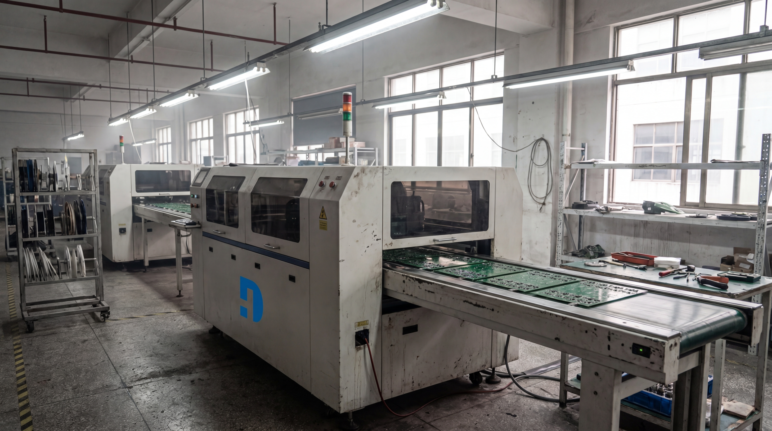
How Does A Circuit Board Pattern Become A Manufactured PCB?
The Designer Creates The Layout In EDA Software, Verifies Electrical And Manufacturing Rules, Then Exports Production Files.
The PCB Manufacturer Uses These Files To Form Copper Layers, Drill Holes, Plate Vias, Apply Solder Mask, Add Surface Finish, Print Markings, And Inspect The Finished Board.
What Files Are Needed To Manufacture A Circuit Board Pattern?
A Complete Production Package Helps Avoid Quotation Delays And Manufacturing Errors.
| File Or Information | Purpose |
| Gerber Or Fabrication Data | Defines Copper, Mask, And Silkscreen Layers |
| Drill Files | Defines Plated And Non-Plated Holes |
| Board Outline | Confirms Final Shape And Dimensions |
| Layer Stack-Up | Defines Materials And Copper Structure |
| Impedance Requirements | Supports Controlled Signal Performance |
| Fabrication Drawing | Lists Board Specifications |
| BOM | Required For PCB Assembly |
| Pick-And-Place File | Required For Automated Component Placement |
| Assembly Drawing | Helps Verify Component Orientation |
| Test Requirements | Defines Inspection Or Functional Validation |
What Should Buyers Ask Before Ordering A PCB Pattern Design?
Many General Guides Explain Traces And Pads, But Buyers Also Need Clear Manufacturing Answers.
Can The Pattern Be Produced At The Required Volume?
A Prototype Pattern May Be Easy To Build Once But Difficult To Repeat In Larger Batches.
Confirm Material Availability, Process Capability, Inspection Requirements, And Production Tolerance Before Scaling.
Does The Pattern Need DFM Review Before Fabrication?
Yes. A DFM Review Helps Identify Trace, Pad, Clearance, Drill, Mask, Panelization, And Assembly Issues Before They Become Physical Defects.
Does The Board Need Controlled Impedance?
It May Be Required For High-Speed Digital, RF, Communication, Or Differential Signal Designs.
The Manufacturer Needs The Stack-Up, Target Impedance, Copper Requirements, And Relevant Net Information Before Production.
Which Test Is Suitable For The Board?
Bare PCBs Commonly Require Electrical Connectivity Testing. Assembled Boards May Need AOI, X-Ray, Functional Testing, Or Other Checks.
The Right Test Plan Depends On The Board Complexity, Component Type, Product Risk, And Application.
How Can A Designer Reduce PCB Manufacturing Cost?
Start With A Manufacturable Stack-Up, Avoid Unnecessary Complexity, Use Verified Footprints, Limit Excessively Tight Rules, And Submit Complete Files.
Lower Cost Should Not Come From Removing Necessary Signal, Thermal, Safety, Or Quality Controls.
Circuit Board Patterns For Telecommunications And Networking
Telecommunications Products Need Reliable Signal Transfer, Stable Timing, Low Noise, And Efficient Power Delivery.
A High-Speed PCB Layout For Network Equipment May Use Multilayer Boards, Controlled Impedance Traces, Differential Pairs, Continuous Ground Planes, And Carefully Managed Power Distribution.
Circuit Board Patterns For RF And Wireless Products
RF And Microwave Designs Depend Strongly On Physical Trace Shape, Reference Ground, Impedance, Connector Placement, And Material Selection.
An RF Circuit Board Pattern Must Minimize Unwanted Reflections And Signal Loss While Supporting Stable Wireless Performance.
Circuit Board Patterns For Automotive And Industrial Electronics
Automotive And Industrial Boards May Face Vibration, Temperature Changes, Electrical Noise, And Long Operating Periods.
For These Projects, The Pattern Should Support Reliable Power Paths, Stable Connections, Suitable Clearance, Thermal Control, And Clearly Defined Testing Requirements.
Circuit Board Patterns For IoT And Compact Devices
IoT Products Often Combine Wireless Signals, Sensors, Power Conversion, Microcontrollers, And Compact Mechanical Space.
A Well-Planned PCB Layout Pattern Helps Separate Sensitive Signals, Manage Antenna Areas, Reduce Noise, And Fit More Functions Into A Smaller Product.
Frequently Asked Questions About Circuit Board Patterns
What Is The Purpose Of A Circuit Board Pattern?
A Circuit Board Pattern Defines The Conductive Connections That Carry Signals And Power Between Components On A PCB.
Is A PCB Pattern Only A Visual Design?
During Layout, It Is A Digital Representation Of Copper Geometry. After Fabrication, The Approved Pattern Becomes Physical Conductive Copper On The Board.
What Is The Difference Between A Trace And A Pad?
A Trace Carries Electrical Signals Or Power Across The PCB. A Pad Provides The Copper Connection Point Where A Component Lead Or Pin Is Soldered.
What Does A Via Do In A PCB Pattern?
A Via Creates An Electrical Connection Between Copper Layers, Allowing Signals, Power, Or Heat To Move Through The Board Structure.
Why Are Ground Planes Important?
Ground Planes Provide Low-Impedance Return Paths, Help Reduce Noise, Support Signal Integrity, And Improve EMI Performance.
When Should Designers Use Differential Pair Routing?
Differential Pair Routing Is Commonly Used For High-Speed Or Noise-Sensitive Interfaces That Need Balanced Signal Paths And Controlled Electrical Behavior.
Why Is DFM Important For Circuit Board Patterns?
DFM Helps Confirm That The Pattern Can Be Reliably Manufactured And Assembled Without Avoidable Defects, Delays, Or Rework.
What Files Should Be Sent For PCB Manufacturing?
A Manufacturer Commonly Needs Gerber Or Equivalent Fabrication Data, Drill Files, Board Specifications, Stack-Up Requirements, And Testing Information.
For Assembly, The Buyer Should Also Provide A BOM, Pick-And-Place File, And Assembly Drawing.
Choose A Manufacturable Circuit Board Pattern For Your PCB Project
A Reliable Circuit Board Pattern Must Do More Than Connect Components On A Screen. It Must Support Signals, Power, Heat, Assembly, Testing, And Repeatable Production.
For Custom PCB Projects, Haode PCBA Can Review Your Manufacturing Files And Help Turn A Verified Printed Circuit Board Layout Into A Production-Ready PCB Or PCBA Solution.