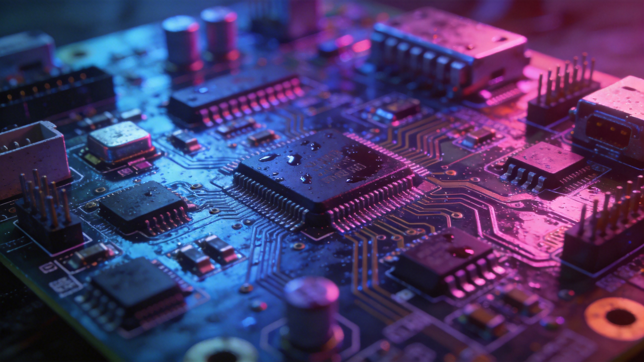
Printed Circuit Boards—often called PCBs, circuit boards, printed wiring boards (PWB), or electronic boards—are the foundational platform that mechanically supports components and electrically connects them using copper traces on an insulating base material. In simple terms, a PCB is the “signal highway” that routes power and data between parts so electronic devices work reliably. Understanding Printed Circuit Boards (PCBs)
How Printed Circuit Boards Work
A printed circuit board replaces bulky point-to-point wiring with engineered copper pathways. These conductive pathways (also known as tracks or traces) form controlled routes for current and signals, improving consistency, reducing noise, and making electronics easier to assemble and test.
Core PCB Parts
- Traces / Tracks / Copper Paths: Conductive routes that connect components
- Pads / Solder Pads / Land Patterns: Exposed metal areas where parts are soldered
- Vias / Plated Through Holes (PTH) / Interlayer Connections: Conductive holes that link layers together
- Silkscreen / Legend / Markings: Printed labels for reference designators, polarity, and assembly guidance
Main Types Of Printed Circuit Boards
Most buyers start by choosing the PCB layer count. The three common options are:
1) Single-Layer PCB (Single-Sided Circuit Board)
A single-sided PCB has copper on one side. It’s cost-effective for simple circuits and high-volume products.
2) Double-Layer PCB (Double-Sided Printed Circuit Board)
A double-sided PCB has copper on both sides and uses vias to connect layers. It fits moderate complexity designs.
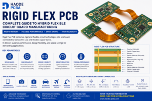
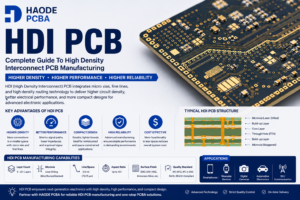
3) Multi-Layer PCB (Multilayer Circuit Board)
A multilayer PCB stacks multiple copper layers separated by dielectric insulation, enabling higher routing density, better signal integrity, and compact layouts.
Quick Comparison Table
| PCB Type | Also Called | Best For | Key Advantage |
|---|---|---|---|
| Single-Layer | Single-Sided PCB | Simple electronics, low-cost products | Lowest cost, easy fabrication |
| Double-Layer | Double-Sided PCB | Mid-complexity control boards | More routing space, flexible layout |
| Multi-Layer | Multilayer PCB | High-density, high-speed designs | Compact routing + improved performance |
Printed Circuit Board Manufacturing Process (From Design To Reality)
A professional PCB workflow typically includes PCB fabrication (building the bare board) and PCB assembly (mounting components).
Step 1: PCB Fabrication (Bare Board Manufacturing)
Fabrication converts design data into a physical board using processes such as etching, drilling, and layer lamination (for multilayer boards).
Common fabrication keywords (for SEO coverage):
Bare PCB, PCB manufacturing, PCB board fabrication, copper etching, drilling, lamination, solder mask, surface finish (ENIG / HASL), impedance control (if needed).
Step 2: PCB Assembly (PCBA)
PCB assembly—also called PCBA, circuit board assembly, or electronics assembly—places and solders components onto the board, often with automation for speed and repeatability.
Component Mounting Methods: Through-Hole vs SMT
Your assembly method affects cost, reliability, and component choices.
Through-Hole Technology (THT)
Through-hole mounting inserts component leads into drilled holes and solders them on the opposite side—great for connectors, high-strength parts, and harsh environments.
Surface Mount Technology (SMT)
SMT (surface mount assembly) mounts components directly onto the PCB surface using solder paste and reflow soldering—ideal for dense layouts and modern electronics.
PCB Design Considerations That Impact Quality
A board that works in CAD can still fail in real-world applications if designers ignore critical PCB layout rules. Key considerations include:
- Trace width & spacing (current capacity, manufacturability, creepage/clearance)
- Via placement & stackup planning (routing efficiency, reliability)
- Component placement (thermal behavior, assembly yield, serviceability)
- Signal integrity (noise control, crosstalk reduction, stable high-quality signals)
PCB Testing & Inspection
To confirm build quality, manufacturers use inspection and test methods like:
- AOI (Automated Optical Inspection) for visual solder joint and placement verification
- ICT (In-Circuit Testing) to check opens/shorts and component-level integrity
Depending on product risk, teams may also add functional testing, X-ray (for BGAs), or reliability screening.
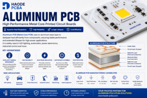
Printed Circuit Board Applications
Printed circuit boards power everything from everyday consumer products to high-reliability systems, including industrial equipment and aerospace-grade electronics.