PCB, Or Printed Circuit Board, Is One Of The Most Important Foundations In Modern Electronics. From Consumer Devices And Industrial Equipment To Automotive Systems And Medical Products, Almost Every Electronic Application Depends On A Reliable Circuit Board To Connect And Support Its Components.
Although PCB Boards Are Used Everywhere, Many People Still Ask The Same Basic Questions. What Is A PCB? How Does A Printed Circuit Board Work? What Materials Are Used In A PCB Circuit Board? And What Is The Difference Between PCB Manufacturing And PCB Assembly?
This Guide Covers The Essential PCB Basics In A Clear And Practical Way. You Will Learn What A Printed Circuit Board Is, How It Is Built, Common PCB Terms, The Main Types Of PCB, How Components Are Assembled, And What Beginners Should Know Before Starting A PCB Design Project.
What Is A PCB?
A PCB Is A Flat Board That Mechanically Supports And Electrically Connects Electronic Components Through Copper Traces, Pads, And Conductive Pathways. Instead Of Using Loose Wires To Connect Different Parts Of A Circuit, A Printed Circuit Board Uses An Organized Layout That Is More Compact, More Reliable, And Easier To Manufacture.
A PCB Board Is Also Called A Printed Circuit Board, Circuit Board, Printed Wiring Board, Electronic Circuit Board, Or PCB Circuit Board. Although These Terms Are Similar, PCB And Printed Circuit Board Remain The Most Commonly Used Names In The Electronics Industry.
The Main Purpose Of A PCB Is To Route Signals And Power Between Electronic Components While Providing A Stable Physical Platform For Assembly. That Is Why Custom PCB Boards Are Essential In Modern Electronic Product Development.
Why PCB Basics Matter
Understanding PCB Basics Is Important For Engineers, Buyers, Students, Product Developers, And Sourcing Teams. Whether You Are Learning Electronics, Comparing PCB Assembly Services, Or Selecting A PCB Manufacturer, It Is Essential To Understand How A Circuit Board Is Structured And How It Performs.
A Good Understanding Of PCB Basics Also Helps When Discussing PCB Design, PCB Fabrication, PCB Assembly, PCB Prototype Development, Multilayer PCB Design, Surface Mount Technology, Through-Hole Assembly, And FR4 PCB Materials.
For SEO Independent Websites, PCB Basics Is Also A Strong Informational Keyword Because It Connects Naturally To Many Related Long-Tail Searches.
What Is A PCB Made Of?
A Printed Circuit Board Is Built From Multiple Layers Of Materials Laminated Together. Each Layer Has A Specific Job, And Together They Create A Durable And Functional Electronic Circuit Board.
FR4 Substrate
The Base Of Most Rigid PCB Boards Is Made From FR4, A Fiberglass-Reinforced Epoxy Material. This Substrate Gives The Board Its Strength, Thickness, Insulation, And Mechanical Stability.
FR4 PCB Material Is Widely Used Because It Offers A Strong Balance Of Electrical Insulation, Durability, Heat Resistance, And Cost Effectiveness. While FR4 Is The Most Common Option, Some Designs Use Flexible Materials For Flexible PCB Applications.
Copper Layer
On Top Of The Substrate, A Thin Copper Foil Is Laminated To The Board Surface. This Copper Forms The PCB Traces, Pads, Planes, And Conductive Pathways That Carry Current And Signals.
Depending On The Product, The Board May Be A Single-Sided PCB, Double-Sided PCB, Or Multilayer PCB. Copper Thickness Can Also Vary Depending On Current Requirements And Application Needs.
Solder Mask
The Solder Mask Is The Protective Layer Applied Over Most Of The Copper Surface. It Prevents Accidental Short Circuits, Protects The Copper From Corrosion, And Helps Control Solder Flow During PCB Assembly.
Green Is The Most Common Solder Mask Color, But Red, Blue, White, Black, And Other Custom Colors Are Also Available.
Silkscreen
The Silkscreen Is The Printed Label Layer On The Surface Of The PCB Board. It Usually Includes Reference Designators, Pin Labels, Component Outlines, Symbols, Logos, And Polarity Marks.
A Clear PCB Silkscreen Helps Technicians Assemble, Inspect, And Troubleshoot The Board More Easily.
How Does A PCB Work?
A Printed Circuit Board Works By Creating Electrical Connections Between Components Through Copper Traces And Other Conductive Features. Once Electronic Parts Are Mounted And Soldered To The Board, The PCB Circuit Allows Current And Signals To Move Between Them In A Controlled And Reliable Way. For Example, Power May Travel Through A Copper Trace From A Connector To A Voltage Regulator, Then Continue To An Integrated Circuit, Sensor, Or Output Device. In This Way, The Board Layout Determines How These Connections Are Made, How Signals Are Routed, And How The Circuit Performs Electrically. Therefore, A Well-Designed PCB Circuit Board Is Not Just A Mechanical Support Board. Instead, It Also Plays A Critical Role In System Performance, Signal Integrity, Thermal Behavior, And Manufacturing Reliability.
Common Types Of PCB
There Are Several Common PCB Types, And The Right Choice Depends On Cost, Complexity, Available Space, And Performance Requirements.
Single-Sided PCB
A Single-Sided PCB Has One Copper Layer On One Side Of The Substrate. It Is Simple, Affordable, And Often Used In Basic Or Low-Cost Electronics.
Double-Sided PCB
A Double-Sided PCB Has Copper On Both Sides Of The Board. It Offers More Routing Flexibility And Is Common In Many Standard Electronic Products.
Multilayer PCB
A Multilayer PCB Uses Multiple Copper Layers Stacked Together. This Type Of Printed Circuit Board Is Commonly Used In Advanced Electronics That Require Compact Design, High Component Density, And Complex Signal Routing.
Rigid PCB
A Rigid PCB Uses Solid Materials Such As FR4 And Does Not Bend During Normal Use. This Is The Most Common PCB Type In Standard Electronics Manufacturing.
Flexible PCB
A Flexible PCB Uses Bendable Base Materials And Is Suitable For Compact Devices, Wearable Electronics, And Applications With Limited Internal Space.
Rigid-Flex PCB
A Rigid-Flex PCB Combines Rigid And Flexible Sections In One Design. It Is Often Used In High-Performance, Space-Constrained, Or High-Reliability Products.
Essential PCB Terminology
When Dealing With PCB Manufacturing Or PCB Assembly, You Will Often Hear Technical Terms. Understanding These Terms Is Part Of Learning Solid PCB Basics.
Trace
A Trace Is A Narrow Copper Path On The Board That Carries Electrical Current Or Signals.
Pad
A Pad Is The Exposed Metal Area Where A Component Lead Or Terminal Is Soldered.
Via
A Via Is A Hole That Passes A Signal From One Copper Layer To Another In A Multilayer PCB.
Plated Through Hole
A Plated Through Hole, Or PTH, Is A Hole With Conductive Plating Through The Board. It May Be Used For Through-Hole Components Or Signal Transfer Between Layers.
Plane
A Plane Is A Large Area Of Copper, Usually Used For Ground Or Power Distribution.
Annular Ring
The Annular Ring Is The Copper Ring Around A Drilled Hole. It Is Important For Mechanical Strength And Electrical Connection Reliability.
PCB Solder Paste
Solder Paste Is A Mixture Of Solder Particles And Flux Used In Surface Mount PCB Assembly Before Reflow Soldering.
Solder Mask
The Solder Mask Is The Protective Coating That Covers Most Copper Features While Leaving Solder Pads Exposed.
Silkscreen
The Silkscreen Provides Printed Labels And Symbols On The Board Surface For Identification And Easier Assembly.
Thermal Relief
A Thermal Relief Is A Connection Style Used Between A Pad And A Plane To Improve Solderability.
Slot
A Slot Is A Non-Round Hole Or Opening In The Board. Some Slots Are Plated, And Some Are Non-Plated Depending On The Design Requirement.
DRC
DRC, Or Design Rule Check, Is A Software-Based Verification Process Used During PCB Layout Design To Detect Spacing, Trace Width, Drill, And Connectivity Issues Before Fabrication.
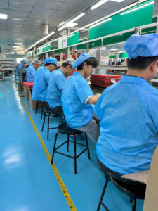
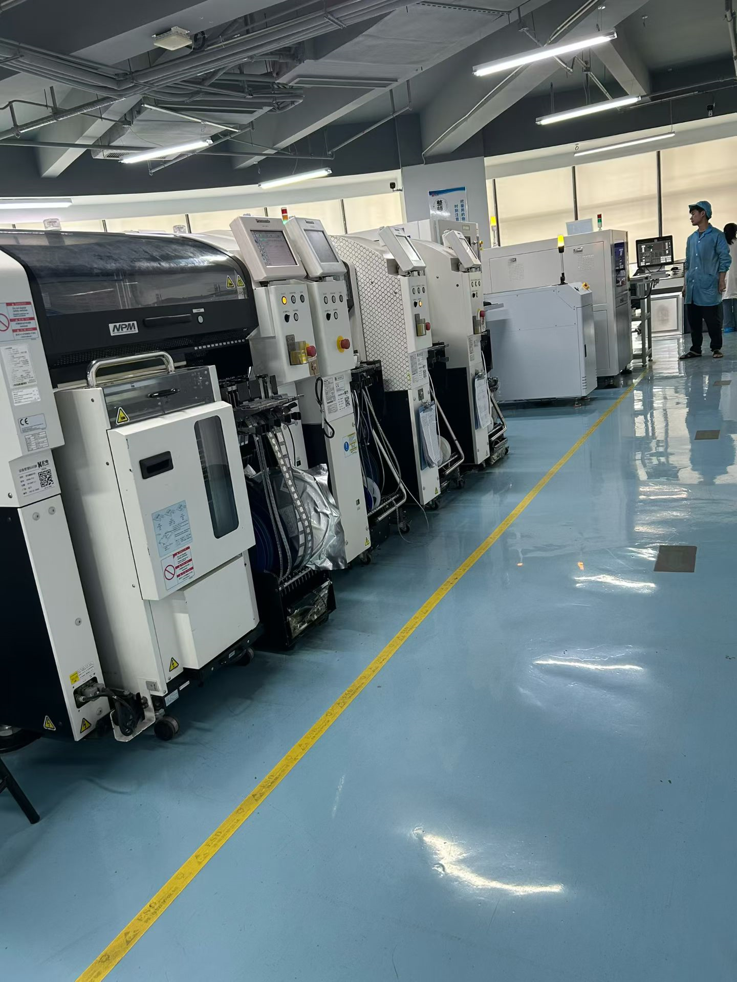
PCB Assembly Basics
Bare Printed Circuit Board Only Becomes Functional After Technicians Mount And Solder Electronic Components Onto It. At This Stage, The Board Turns Into A Working Electronic Assembly. This Process Is Known As PCB Assembly, Or PCBA. In Modern Electronics, There Are Two Main Assembly Methods, And Each One Supports Different Component Types, Product Designs, And Manufacturing Needs.
Through-Hole PCB Assembly
In Through-Hole PCB Assembly, Technicians Insert Component Leads Through Drilled Holes And Then Solder Them On The Opposite Side Of The PCB. As A Result, This Assembly Method Creates Strong Mechanical Bonding And Delivers Excellent Durability. For This Reason, It Is Widely Used For Connectors, Large Components, And Many Industrial Electronic Products Where Higher Mechanical Strength And Long-Term Reliability Are Essential.
Surface Mount PCB Assembly
In Surface Mount PCB Assembly, Also Called SMT PCB Assembly, Technicians Mount Components Directly On The PCB Surface Pads.
Many Modern Products Use A Mixed Approach That Combines SMT Assembly And Through-Hole Assembly.
Main Steps In The PCB Assembly Process
The PCB Assembly Process Usually Includes Several Key Stages.
Solder Paste Printing
A Stencil Is Used To Apply Solder Paste Accurately To The Surface Mount Pads.
Pick And Place
A Pick-And-Place Machine Places Electronic Components Onto The Board In Their Correct Positions.
Reflow Soldering
During Reflow Soldering, The Solder Paste Melts And Forms Electrical And Mechanical Joints Between The Components And The Pads.
Through-Hole Soldering
If The Design Includes Through-Hole Parts, They May Be Soldered By Hand, Wave Soldering, Or Selective Soldering.
Inspection And Testing
After Assembly, Technicians Inspect And Test The PCBA Board To Check Soldering Quality, Detect Shorts And Open Circuits, And Identify Placement Errors.
PCB Design Basics
Learning PCB Basics Also Means Understanding The Fundamentals Of PCB Design. In Other Words, A Good PCB Layout Does More Than Simply Connect Components. It Must Also Consider Manufacturability, Signal Routing, Thermal Performance, Component Spacing, And Assembly Efficiency, So The Final PCB Can Perform Better Throughout Design, Production, And Use.
A Strong PCB Design Typically Includes A Clear Schematic, Proper Trace Widths, Suitable Pad And Hole Sizes, Correct Layer Stackup, Practical Component Placement, Reliable Grounding And Power Routing, And Manufacturable Output Files.
Before Production, Designers Usually Run A Design Rule Check To Make Sure The Layout Meets The Required Manufacturing Rules.
Tips For Beginners In PCB Design
If You Are New To Printed Circuit Board Design, First, Start With A Strong Schematic, Because It Builds The Foundation For A Reliable PCB Layout. Next, Choose Suitable PCB Design Software, Since Different Tools Offer Different Libraries, Design Functions, And Export Options. In Addition, Reviewing Existing PCB Layouts Can Help You Better Understand Routing, Component Placement, And Manufacturability. More Importantly, You Should Think About Production Early, Because A Good Custom PCB Design Should Not Only Work Electrically, But Also Support Smooth Fabrication, Efficient Assembly, Accurate Inspection, And Reliable Testing. Finally, Keep Practicing, Because PCB Design Skills Improve Over Time Through Repetition, Careful Review, And Continuous Optimization.
PCB Vs PCBA
Many Buyers Confuse PCB And PCBA, But They Are Not The Same.
A PCB Refers To The Bare Printed Circuit Board Without Any Mounted Components.
A PCBA Refers To The Finished Printed Circuit Board Assembly After Technicians Install And Solder The Components.
This Difference Is Important When Searching For PCB Manufacturing, PCB Fabrication, PCB Assembly Services, Turnkey PCBA, Or Custom PCB And Assembly.
Conclusion
PCB Basics Covers The Essential Knowledge You Need To Understand How A Printed Circuit Board Is Designed, Built, And Used In Modern Electronics. A PCB Board Provides The Structure And Electrical Connections That Allow Components To Function Together In A Compact, Reliable, And Manufacturable Form.
From FR4 Substrate, Copper Traces, Solder Mask, And Silkscreen To PCB Assembly, SMT, Through-Hole Technology, And PCB Design, Every Part Of The Process Plays A Role In Overall Product Quality.
Whether You Are A Beginner, A Sourcing Buyer, Or A Company Providing PCB Manufacturing And PCB Assembly Services, Understanding These PCB Basics Is The First Essential Step, Because It Helps Improve Design Decisions, Strengthens Communication Efficiency, And Ultimately Leads To Better Electronic Products.