Complete Guide To PCB Design Process
Designing PCB board (Printed Circuit Board) is the foundation of every modern electronic product. From consumer electronics and IoT devices to industrial equipment and automotive systems, proper PCB board design ensures electrical performance, signal integrity, and manufacturing reliability.
Understanding how to design a PCB board involves several critical steps including schematic creation, component selection, PCB layout, routing, and design rule verification. A well-designed printed circuit board layout reduces production costs, improves signal stability, and ensures smooth PCB assembly (PCBA manufacturing).
In this guide, we explain the Complete PCB design workflow, essential tools, best practices, and professional strategies used by engineers in modern electronics development.
What Is PCB Board Design?
PCB board design refers to the process of creating the electronic layout and physical structure of a printed circuit board that connects electronic components through conductive copper traces.
A typical PCB design process includes two major stages:
- Schematic Design
- PCB Layout Design
The schematic defines the logical electrical connections, while the PCB layout defines the physical placement of components and routing of copper traces on the circuit board.
A properly engineered PCB circuit board design ensures:
- Reliable electrical connectivity
- Stable signal transmission
- Efficient heat dissipation
- Compatibility with PCB assembly processes
Without careful PCB design planning, a circuit that works in simulation may fail during real-world manufacturing or operation.
Essential PCB Design Software
Modern PCB board design relies on professional electronic design automation (EDA) tools.
Common PCB design software includes:
| PCB Design Tool | Features |
|---|---|
| Altium Designer | Professional high-speed PCB design |
| KiCad | Open-source PCB layout software |
| Eagle PCB | Popular for small electronics projects |
| OrCAD | Advanced enterprise PCB design |
| EasyEDA | Web-based PCB design platform |
These tools help engineers create schematics, PCB layouts, component libraries, and manufacturing files such as Gerber files.
Step-By-Step Guide: How To Design A PCB Board
Designing a PCB board follows a structured engineering workflow.
Step 1: Define Circuit Requirements
Before starting PCB design, engineers must clearly define the functional requirements of the circuit board.
Important considerations include:
- Power supply voltage
- Signal type (analog, digital, RF)
- Current requirements
- Operating environment
- Size limitations
These parameters determine the PCB architecture, layer stack-up, and component selection.
Step 2: Create The Circuit Schematic
The schematic diagram is the logical representation of how electronic components connect electrically.
During schematic design engineers:
- Select electronic components
- Define electrical connections
- Assign component values
- Add power and ground networks
A clear and accurate schematic ensures the printed circuit board functions correctly before layout begins.
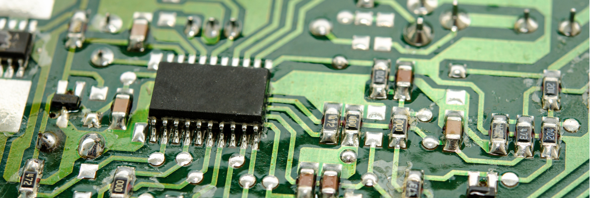
Step 3: Select PCB Components And Footprints
Each component must be linked to a PCB footprint, which defines the physical pads used during PCB assembly.
Typical components include:
- Integrated circuits (ICs)
- Resistors
- Capacitors
- Connectors
- Diodes
- Transistors
Proper footprint selection ensures compatibility with SMT PCB assembly or through-hole PCB manufacturing.
Step 4: Plan The PCB Layout
PCB layout planning determines component placement and board structure.
Key layout considerations include:
- Board size and shape
- Layer stack-up design
- Power distribution network
- Thermal management
- EMI and signal integrity
Engineers usually place critical components first, such as processors, power regulators, and connectors.
Strategic component placement simplifies routing and improves PCB performance and manufacturability.
Step 5: Route PCB Traces
Routing is the process of creating copper traces that electrically connect components.
Routing guidelines include:
- Keep traces as short as possible
- Avoid sharp angles (use 45° routing)
- Separate analog and digital signals
- Maintain impedance control for high-speed signals
Good routing practices improve signal integrity, noise control, and electrical reliability.
Step 6: Design Power And Ground Planes
Efficient power distribution and grounding are critical for stable PCB operation.
Most modern PCBs include:
- Dedicated ground planes
- Power planes
- Decoupling capacitors near ICs
These design strategies reduce electrical noise, voltage drop, and electromagnetic interference (EMI).
Step 7: Perform PCB Design Rule Check (DRC)
Before manufacturing, engineers must run Design Rule Checks (DRC) to detect layout errors.
DRC verifies:
- Minimum trace width
- Spacing between traces
- Pad and via sizes
- Clearance rules
Passing DRC ensures the PCB design meets manufacturing capabilities and PCB fabrication standards.
Step 8: Generate Manufacturing Files
Once the PCB design is complete, the final step is exporting files required for PCB fabrication and assembly.
Typical manufacturing files include:
- Gerber files
- Drill files
- Bill of Materials (BOM)
- Pick and place files
- Assembly drawings
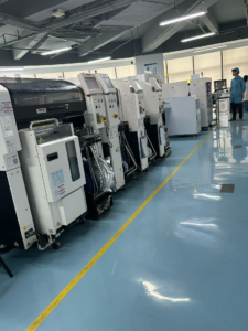
These files allow PCB manufacturers to produce and assemble the printed circuit board assembly (PCBA).
Common PCB Design Types
Different electronic applications require different PCB board structures.
| PCB Type | Description |
|---|---|
| Single-Sided PCB | One copper layer, simple electronics |
| Double-Sided PCB | Two copper layers |
| Multilayer PCB | Complex circuits with multiple layers |
| Flexible PCB | Bendable circuit boards |
| Rigid-Flex PCB | Combination of rigid and flexible boards |
High-performance electronics often require multilayer PCB designs for signal routing and power distribution.
PCB Design Best Practices
Professional PCB engineers follow several best practices to improve PCB performance and reliability.
Keep Signal Paths Short
Shorter traces reduce signal delay, noise, and electromagnetic interference.
Separate Analog And Digital Circuits
Mixing sensitive analog signals with high-speed digital signals may cause signal distortion.
Optimize Thermal Management
Heat-producing components should have:
- Thermal vias
- Copper pours
- Heat sinks
Proper thermal design improves electronic product reliability.
Follow Manufacturability Guidelines
Design for manufacturability (DFM) ensures the PCB design can be efficiently fabricated and assembled.
PCB Design Applications
Modern PCB board design powers nearly every electronic device.
Major industries include:
- consumer electronics
- automotive electronics
- industrial automation
- telecommunications equipment
- aerospace systems
- medical devices
As electronics continue to evolve, advanced PCB layout design and high-speed circuit board engineering become increasingly important.
Conclusion
Learning how to design a PCB board is a crucial skill for electronics engineers and product developers. A well-structured PCB design process, including schematic development, component placement, routing, and verification, ensures reliable electronic performance and efficient manufacturing.
By following professional PCB design practices and using modern design tools, engineers can create high-performance printed circuit boards that support advanced electronics, scalable production, and long-term product reliability.