High Speed PCB Design Haode Refers To Advanced Printed Circuit Board Engineering Used To Support Fast Signal Transmission, Stable Circuit Performance, And Reliable Electronic Product Development. As Electronic Systems Continue To Move Toward Higher Frequencies, Faster Data Rates, And More Compact Layouts, High-Speed PCB Design Has Become A Critical Part Of Modern Hardware Engineering. Companies Focused On End-To-End Product Development, Such As Haode, Treat PCB Design As A Core Part Of Turning Complex Electronic Ideas Into Manufacturable Products.
In High-Speed Electronics, A PCB Is No Longer Just A Mechanical Platform For Components. It Becomes An Active Part Of Signal Integrity, Power Stability, Electromagnetic Control, And System Reliability. Poor Layout Decisions Can Cause Reflection, Crosstalk, Timing Errors, EMI Problems, And Product Instability. That Is Why High-Speed PCB Design Requires Careful Planning From Schematic Capture To Stackup Definition, Routing Strategy, Simulation, And Manufacturing Review. High Speed PCB Design Haode Emphasizes Controlled Impedance, Signal Integrity, EMI Control, And Precision Layout As Essential Priorities.
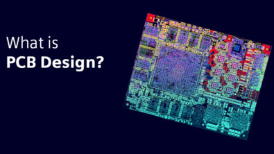
What Is High-Speed PCB Design?
High-Speed PCB Design Is The Process Of Creating A Printed Circuit Board For Signals Fast Enough That Transmission Line Effects Must Be Considered. In These Designs, Trace Width, Trace Length, Layer Stackup, Ground Reference, Dielectric Properties, Via Structures, And Component Placement All Affect Electrical Performance.
This Means The Designer Must Think Beyond Simple Connectivity. A Trace Is Not Just A Copper Path. In A High-Speed Circuit, It Acts Like A Controlled Transmission Line. If The Impedance Changes Unexpectedly Or The Return Path Is Broken, Signal Quality Can Degrade Very Quickly. That Is Why High-Speed PCB Design Is Closely Connected To Controlled Impedance PCB Design, Signal Integrity PCB Layout, And EMI Aware Circuit Board Engineering.
Why High-Speed PCB Design Matters
High-Speed PCB Design Matters Because Modern Electronic Products Depend On Fast, Clean, And Predictable Signal Transmission. High-Speed Boards Are Common In Communication Equipment, Embedded Systems, Industrial Electronics, Medical Devices, Aerospace Hardware, And Advanced Consumer Products.
When High-Speed Rules Are Ignored, A Product May Suffer From Data Errors, Poor EMC Performance, Random Failures, Certification Problems, And Expensive Redesign Cycles. A Well Designed High-Speed PCB Improves Signal Clarity, Reduces Error Rates, Supports Regulatory Compliance, And Helps A Product Move More Smoothly From Prototype To Production.
Stackup Planning In High-Speed PCB Design
A Strong PCB Stackup Is One Of The Most Important Parts Of High-Speed Board Design. Layer Arrangement Affects Impedance Control, Return Current Flow, EMI Behavior, Power Integrity, And Routing Efficiency.
A Good High-Speed Stackup Usually Includes Solid Reference Planes, Carefully Planned Signal Layers, And Controlled Spacing Between Conductors And Reference Planes. Designers Often Use Microstrip Or Stripline Routing Structures Depending On The Required Performance And Density. Continuous Ground Reference Is Especially Important Because Return Current Needs A Stable Path To Minimize Loop Area And Reduce EMI.
Controlled Impedance And Signal Integrity
Controlled Impedance Is A Core Requirement In High-Speed PCB Design. Fast Digital And RF Signals Must Travel Through Traces With Predictable Electrical Characteristics. If Trace Geometry Or Reference Conditions Change, Reflection And Distortion Can Occur.
To Achieve Controlled Impedance, Engineers Must Coordinate Trace Width, Copper Thickness, Dielectric Constant, Dielectric Height, And Reference Plane Distance. This Is Why High-Speed PCB Layout Cannot Be Separated From Stackup Engineering. A Board House And Design Team Must Work Together Early To Make Sure The Final Fabricated PCB Matches The Intended Electrical Performance.
Differential Pair Routing And Length Matching
Many High-Speed Interfaces Use Differential Signals Because They Help Improve Noise Immunity And Support Faster Data Transfer. In These Cases, The Two Traces Must Be Routed As A Controlled Pair With Stable Spacing And Similar Electrical Length. Poor Differential Pair Layout Can Increase Skew, Reduce Signal Quality, And Harm Timing Performance.
Length Matching Is Also Important In Buses Such As DDR Memory Interfaces, Where Signals Must Arrive Within Tight Timing Windows. Trace Matching Does Not Mean Every Trace Must Be Identical, But Critical Nets Must Be Balanced According To Interface Requirements. High-Speed PCB Design Therefore Requires Discipline In Topology Planning, Trace Tuning, And Delay Control.
Power Integrity And Decoupling Strategy
A High-Speed Board Needs More Than Clean Signal Routing. It Also Needs Stable Power Delivery. Fast ICs Create Sudden Current Demand, And Poor Power Distribution Can Cause Noise, Timing Errors, And Unstable Operation. Good High-Speed PCB Design Uses Low-Impedance Power Distribution Networks, Proper Decoupling Capacitor Placement, And Thoughtful Plane Design To Support Stable Operation.
Decoupling Capacitors Should Be Placed Close To The Power Pins Of High-Speed Devices, And The Current Path Between The Capacitor, Power Pin, And Ground Return Should Be Short And Low Inductance. Power Integrity Becomes Even More Important In Dense Multilayer Boards With Mixed Digital, Analog, And RF Sections.
EMI, EMC, And Return Path Control
High-Speed Signals Can Radiate Noise If Layout Is Poor. That Is Why EMI And EMC Control Are Essential In High-Speed PCB Design. Solid Reference Planes, Short Return Paths, Proper Layer Transitions, And Good Connector Layout Help Reduce Emissions And Improve Compliance Performance.
Designers Must Also Be Careful With Via Transitions, Edge Routing, Clock Placement, And High-Speed Connector Escapes. Every Unnecessary Discontinuity Increases Risk. In High-Speed Products, EMI Control Is Not A Final Fix. It Must Be Built Into The PCB From The Beginning.
Material Selection For High-Speed Boards
Material Selection Has A Direct Effect On Electrical Performance. Standard FR-4 May Work For Many High-Speed Designs, But At Higher Frequencies Or Lower Loss Requirements, Designers May Need Advanced Low-Loss Materials. The Right Material Depends On Operating Frequency, Edge Rate, Thermal Needs, Manufacturing Cost, And Reliability Targets.
For Practical Product Development, Material Choice Must Balance Performance And Manufacturability. A Good Engineering Team Chooses Materials That Support Target Signal Integrity Without Making Production Unnecessarily Complex Or Expensive.
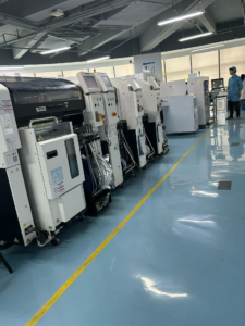
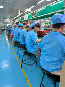
DFM And Transition To Manufacturing
A High-Speed PCB Must Not Only Work In Theory. It Must Also Be Manufacturable. Design For Manufacturability Helps Identify Problems In Footprints, Spacing, Polarity Marks, Test Points, And Process Details Before Boards Enter Production.
This Is Especially Important In High-Speed Designs Because Small Fabrication Variations Can Affect Impedance, Via Quality, And Overall Performance. Design For Manufacturability Helps Reduce Re-Spins, Improve Yield, And Make Prototype Results More Predictable. For Companies Moving From Idea To Product, This Step Is Just As Important As The Initial Layout Work.
Applications Of High-Speed PCB Design
High-Speed PCB Design Is Used In Many Advanced Electronic Products. Common Applications Include Embedded Computing Boards, Wireless Communication Devices, Aerospace Electronics, Medical Instruments, Industrial Automation Systems, And Automotive Electronic Modules.
As Products Continue To Demand Higher Data Rates, Smaller Form Factors, And Greater Reliability, High-Speed PCB Engineering Becomes More Important Across Both Commercial And Industrial Electronics.
Conclusion
High Speed PCB Design Haode Represents A Practical And Engineering Focused Approach To Building Reliable High-Performance Circuit Boards. It Combines Controlled Impedance, Strong Stackup Planning, Stable Return Paths, Power Integrity, EMI Control, And Manufacturable Layout Strategy Into One Complete Development Process.
For Modern Electronic Products, High-Speed PCB Design Is Not Optional. It Is A Core Requirement For Signal Reliability, Product Stability, And Successful Transition From Prototype To Production.