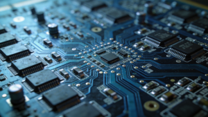
PCB Assembly, also called printed circuit board assembly or circuit board assembly, converts a bare PCB into a functional electronic board.
It achieves this by mounting and soldering components such as resistors, capacitors, ICs, connectors, and functional modules.
In real manufacturing environments, PCB Assembly is far more than simply soldering components onto copper pads.
Instead, it is a controlled production workflow integrating design data, component procurement, soldering processes, inspection stages, and testing procedures.
This structured process ensures the finished PCBA delivers stable performance and high reliability in real-world electronic applications.
What Makes a PCB Assembly “Production-Ready”
Manufacturers consider a board-level assembly production-ready when component placement matches the design intent and solder joints meet acceptance criteria.
They also verify that the assembly successfully passes all required inspections and functional testing procedures before release.
The primary objective is to ensure stable electrical connectivity and predictable thermal behavior during real-world operation.
Equally important, producers aim to maintain consistent mechanical strength and repeatable quality across every production batch.
This requirement applies whether the project involves early-stage prototypes or full-scale mass production runs.
The original article highlights that inspection is critical for validating solder integrity and overall board performance.
Therefore, rigorous inspection becomes the foundation of any reliable PCB Assembly delivery process.
From Design to Custom PCB Assembly: The Practical Workflow
A successful custom PCB Assembly project usually starts with a clean schematic and a manufacturable layout.
Engineers use the schematic to define how parts connect electrically, while they use the PCB layout to determine how the board is physically built, including footprints, routing paths, and placement constraints that directly affect yield, rework rate, and signal integrity.
Once the design is stable, engineers typically run electrical checks and design rule checks to catch missing connections, spacing issues, or layer constraints before releasing manufacturing files.
When the design is ready for fabrication and assembly, you should prepare a complete file package. In most PCB Assembly workflows, the “factory language” is the Gerber set for each layer plus a drill file for holes, then the assembly team also needs BOM and a pick-and-place file to place parts accurately. If you keep these files consistent in revision naming and clearly define alternates, you’ll reduce engineering questions and speed up quoting and production validation.
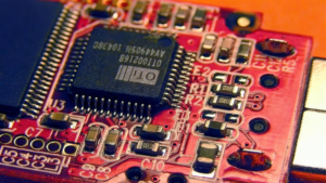
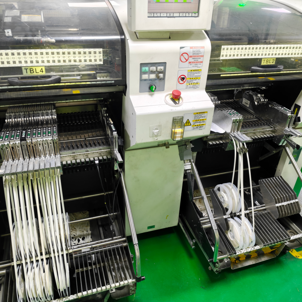
Core PCB Assembly Technologies: SMT, Through-Hole, and Mixed Assembly
Most modern electronics assembly relies on SMT assembly because it supports high-density designs and efficient automation. A typical surface-mount assembly flow includes solder paste printing, solder paste inspection, component placement, reflow soldering, and automated optical inspection.
Manufacturers optimize the SMT production line for speed, consistency, and efficiency, making SMT the dominant technology in high-volume PCBA manufacturing and PCB assembly services.
Through-hole assembly (PTH/THT) is still essential for parts that require stronger mechanical anchoring, higher current handling, or rugged connectors.
In many factories, operators insert leads into plated holes, then use wave soldering or selective soldering depending on board design and component requirements. For mixed-technology assembly, SMT is commonly completed first, followed by through-hole steps, because reflow and wave soldering impose different thermal and process constraints that must be managed carefully to protect components and prevent defects.
Quality Control in PCB Assembly: What Each Inspection Gate Catches
High-yield PCB Assembly depends on “process gates” that detect issues early, when corrections are cheaper and risk is lower.
After solder paste printing, SPI checks whether the paste volume, thickness, and position match the target spec, because poor paste deposits often lead to opens, shorts, tombstoning, or weak joints later in reflow.
In mixed-technology PCB assembly processes, manufacturers usually prioritize SMT placement and reflow soldering before through-hole assembly and wave soldering, since these PCBA manufacturing stages involve different thermal profiles and process requirements that must be tightly managed to ensure component protection, high yield, and defect-free production. Factories also use in-line visual inspection before reflow to catch obvious placement mistakes early, and then AOI after reflow to screen for bridges, offsets, voids, tombstones, and other soldering defects at scale.
For prototypes and first builds, FAI (First Article Inspection) is a strong risk-control step because it validates that the build matches the BOM, placement, and expected component values before scaling to volume.
This is especially useful when a new board is entering pilot production or when you have tight reliability requirements.
Post-Assembly Testing: Electrical Confidence Beyond Visual Quality
Even perfect-looking solder joints do not guarantee correct function, so many projects add electrical checks after the board is built. A simple but powerful method is a multimeter-based continuity/critical node inspection, which relies on planned test pads and can confirm whether key components and nets behave as expected. For higher confidence, functional testing powers the assembled board in a fixture (jig) and verifies real operation under defined conditions, which is often the most meaningful acceptance gate for customer-facing products.
For reliability-sensitive applications, manufacturers may run thermal aging (burn-in) for hours to days to expose early failures and confirm stable operation over time.
In box-build scenarios, a simulation test can validate the assembled product in a usage-like environment before shipment, reducing field returns caused by integration issues.
Benefits of Professional PCB Assembly for OEM and Product Teams
A professionally managed PCB Assembly workflow accelerates the transition from design to shipment by minimizing rework cycles and detecting defects earlier.
This structured approach significantly improves first-pass yield and enhances overall production efficiency.
Over time, it also strengthens cost control by reducing repeated troubleshooting, board scrap, and costly field failures.
These preventive measures help protect delivery schedules and maintain customer confidence.
The source article further emphasizes that assembled circuit boards (PCBA) support a wide range of industries and applications.
Ultimately, dependable PCBA manufacturing, strict quality control, and comprehensive inspection form the foundation for scalable and reliable modern electronic products.
Typical Printed Circuit Board Assembly Applications
PCB and electronics assembly plays a critical role across industrial automation, sensor systems, transportation electronics, medical devices, automotive platforms, aerospace equipment, and consumer electronics.
Each industry focuses on different requirements. Medical electronics demand tighter process control and traceability.
Automotive and aerospace applications require stronger environmental reliability and long-term durability under harsh conditions.
Meanwhile, consumer electronics prioritizes miniaturization, rapid production cycles, and cost-efficient high-volume manufacturing.
Therefore, selecting the appropriate inspection depth and testing strategy should always align with the product’s real-world risk profile and reliability expectations.