
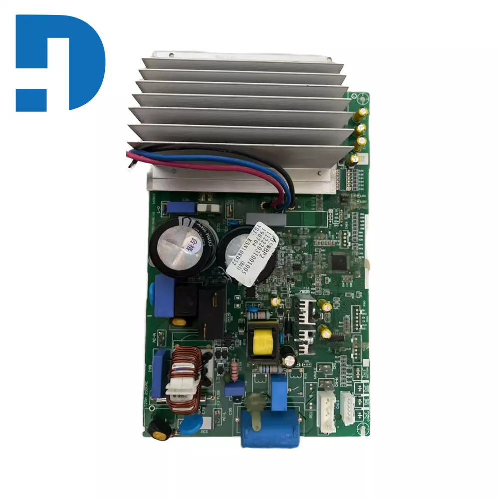
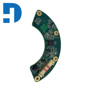
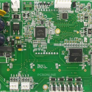
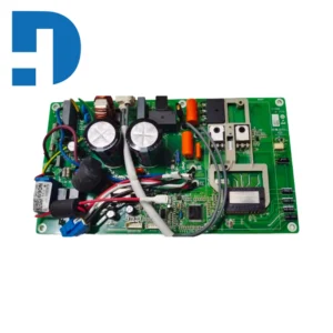
Haode PCBA (Printed Circuit Board Assembly) is a high-reliability core electronic component integrating R&D, design, production and testing. Adopting high-quality FR-4 substrate and high-precision PCB manufacturing process, combined with advanced SMT assembly and DIP insertion technology, it achieves precise soldering and efficient integration of components. The product covers single-sided/double-sided and multi-layer circuit board assembly, supports soldering of precision components such as 0201 ultra-small packages and BGA/QFN, and can adapt to customized needs in various fields including industrial control, consumer electronics, medical equipment, automotive electronics, IoT terminals and new energy.
The production process strictly complies with ISO9001 and IPC-A-610E standards. Through multiple quality control processes such as AOI automatic optical inspection, X-Ray detection, ICT online testing and functional aging testing, it effectively ensures product yield and stability, and reduces the later failure rate. We have a professional engineering and technical team that can provide one-stop services from PCB Layout design, material selection, sample prototyping to mass production. It flexibly responds to customized needs of small batches, multiple batches and fast delivery, helping customers shorten the product R&D cycle and enhance core competitiveness. Whether it is a high-precision industrial control module or a miniaturized consumer electronic motherboard, we can provide customers with customized and cost-effective PCBA solutions relying on mature production processes and strict quality standards.
Assembly Technologies
Surface Mount Technology (SMT): Components are soldered directly onto the board’s surface. SMT is the dominant method due to its efficiency and support for miniaturized designs.
Through-Hole Technology (THT): Leads are inserted into pre-drilled holes. It is still used for components requiring strong mechanical bonds, such as connectors.
Mixed Technology: Combines SMT and THT on a single board, common in complex modern devices.
Core Manufacturing Process
The standard PCBA workflow includes several critical stages:
Solder Paste Stenciling: Applying paste to the board where components will sit.
Pick and Place: Automated machines precisely position components on the paste.
Reflow Soldering: The board passes through an oven to melt the paste and create permanent joints.
Inspection (AOI/X-Ray): Advanced AI-driven Optical Inspection (AOI) and X-ray systems are now standard to detect microscopic flaws.
Functional Testing: The final step to verify that the completed assembly operates according to its design.
Industry Trends
High-Density Interconnect (HDI): Standardized use of 3+N+3 stack-ups and microvias to enable more powerful, compact devices like wearables and 5G hardware.
AI Integration: AI algorithms are now widely used to optimize circuit designs in seconds and monitor smart assembly lines in real-time.
Sustainability: “Green PCB” standards are prevalent, utilizing halogen-free laminates and closed-loop water recycling systems to meet environmental regulations.Rigid-Flex Solutions: Integration of flexible and rigid sections is growing at a CAGR of 6.94%, primarily for automotive and aerospace sectors.
Service Types
Full Turnkey: The manufacturer manages everything, including component sourcing, assembly, and testing.
Consignment/Kitted: The customer provides the components, and the manufacturer performs only the assembly.
 Application Scenario Keywords
- Smart Home PCBA
-
Industrial Control PCBA
-
Automotive Electronics PCBA
-
Medical Equipment PCBA
-
IoT Terminal PCBA
-
New Energy PCBA
-
Smart Home PCBA
 B2B Inquiry CTA
 For export quotations, bulk orders, or project cooperation, Get in Touch with our sales team.
Email: inquiry@devecomponents.com
WhatsApp: +86-15767857371
| Items | Specification |
|---|---|
| Quality Grade | Standard IPC 2 |
| MOQ | 1pc |
| Material | FR-1, FR-2, FR-4, FR4 Halogen Free, CEM-1, CEM-3, Hight TG, Aluminum |
| Available Layers | 1~50 layers |
| Board Thickness (mm) | 0.2mm~7mm |
| Board Thickness Tolerance | ±0.1mm – ±10% |
| Board Side | Min 6*6mm | Max 500*500mm |
| Board Size Tolerance | ±0.1mm – ±0.3mm |
| Copper Thickness | 0.5-4.0oz |
| Copper Thickness Tolerance | +0μm +20μm |
| Copper Weight | 0.5oz – 6.0oz |
| Inner Layer Copper Weight | 0.5oz – 2.0oz |
| Min. Drilled Hole Size | 0.25mm |
| Min. Line Width | 0.075mm (3mil) |
| Min. Line Spacing | 0.075mm (3mil) |
| Surface Treatment | Immersion gold Immersion, HALS/HALS lead free, Chemical tin, Chemical Gold |
| Surface/Hole Plating Thickness | 20μm – 30μm |
| Hole Tolerance | PTH: ±0.075, NTPH: ±0.05 |
| Solder Mask Color | Green/Black/White/Red/Blue/Yellow |
| Solder Mask Sides | As per the file |
| Min Tracing/Spacing | 3mil/3mil |
| Silkscreen Sides | As per the file |
| Silkscreen Color | White, Blue, Black, Red, Yellow |
| Min Annular Ring | 3mil |
| Min Width of Cutout (NPTH) | 0.8mm |
| NPTH Hole Size Tolerance | ±.002″ (±0.05mm) |
| SM Tolerance (LPI) | .003″ (0.075mm) |
| Aspect Ratio | 1.10 (Hole size: Board thickness) |
| PCB Testing | 10V – 250V, flying probe or testing fixture |
| Impedance Tolerance | ±5% – ±10% |
| SMD Pitch | 0.2mm (8mil) |
| BGA Pitch | 0.2mm (8mil) |
| Chamfer of Gold Fingers | 20, 30, 45, 60 |
| Solder Mask Bridge | 0.1mm |
| Minimum Trace / Spacing | 3mil/3mil |
| Minimum trace width in inner layers | ≥ 6 mil To prevent ion migration |
| Minimum distance between vias (plated holes) | 12 ml or higher Prevent ion migration |
| Minimum distance between plated holes and trace | ≥ 12 mil To prevent ion migration |
Reviews
There are no reviews yet.