
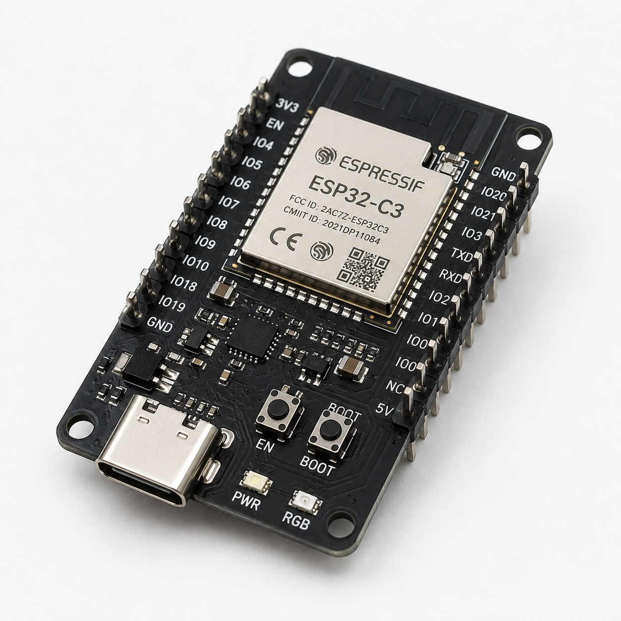
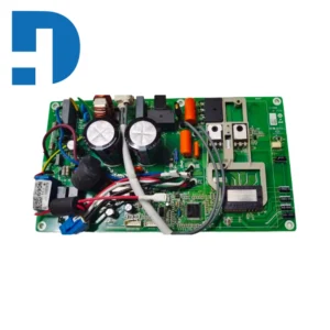
Powerful CPU:ESP32-C3, 32-bit RISC-V single-core processor, running up to 160 MHz
WiFi: 802.11b/g/n protocol, 2.4GhHz,support Station mode, SoftAP mode, SoftAP+Station mode, hybrid mode
Bluetooth:Bluetooth 5.0
Ultra-low power consumption:deep sleep power consumption of about 43ua
Rich board resources:400KB SRAM, 384KB ROM built-in 4M flash
Reliable security features: Encryption hardware accelerators that support AES-128/256, hashing, RSA, HMAC, digital signatures, and secure startup
Onboard led blue light:GPIO8 pin
Package include:
2 x esp32-c3 development board
 Application Scenario Keywords
- Smart Home PCBA
-
Industrial Control PCBA
-
Automotive Electronics PCBA
-
Medical Equipment PCBA
-
IoT Terminal PCBA
-
New Energy PCBA
-
Smart Home PCBA
 B2B Inquiry CTA
 For export quotations, bulk orders, or project cooperation, Get in Touch with our sales team.
Email: inquiry@devecomponents.com
WhatsApp: +86-15767857371
| Items | Specification |
|---|---|
| Quality Grade | Standard IPC 2 |
| MOQ | 1pc |
| Material | FR-1, FR-2, FR-4, FR4 Halogen Free, CEM-1, CEM-3, Hight TG, Aluminum |
| Available Layers | 1~50 layers |
| Board Thickness (mm) | 0.2mm~7mm |
| Board Thickness Tolerance | ±0.1mm – ±10% |
| Board Side | Min 6*6mm | Max 500*500mm |
| Board Size Tolerance | ±0.1mm – ±0.3mm |
| Copper Thickness | 0.5-4.0oz |
| Copper Thickness Tolerance | +0μm +20μm |
| Copper Weight | 0.5oz – 6.0oz |
| Inner Layer Copper Weight | 0.5oz – 2.0oz |
| Min. Drilled Hole Size | 0.25mm |
| Min. Line Width | 0.075mm (3mil) |
| Min. Line Spacing | 0.075mm (3mil) |
| Surface Treatment | Immersion gold Immersion, HALS/HALS lead free, Chemical tin, Chemical Gold |
| Surface/Hole Plating Thickness | 20μm – 30μm |
| Hole Tolerance | PTH: ±0.075, NTPH: ±0.05 |
| Solder Mask Color | Green/Black/White/Red/Blue/Yellow |
| Solder Mask Sides | As per the file |
| Min Tracing/Spacing | 3mil/3mil |
| Silkscreen Sides | As per the file |
| Silkscreen Color | White, Blue, Black, Red, Yellow |
| Min Annular Ring | 3mil |
| Min Width of Cutout (NPTH) | 0.8mm |
| NPTH Hole Size Tolerance | ±.002″ (±0.05mm) |
| SM Tolerance (LPI) | .003″ (0.075mm) |
| Aspect Ratio | 1.10 (Hole size: Board thickness) |
| PCB Testing | 10V – 250V, flying probe or testing fixture |
| Impedance Tolerance | ±5% – ±10% |
| SMD Pitch | 0.2mm (8mil) |
| BGA Pitch | 0.2mm (8mil) |
| Chamfer of Gold Fingers | 20, 30, 45, 60 |
| Solder Mask Bridge | 0.1mm |
| Minimum Trace / Spacing | 3mil/3mil |
| Minimum trace width in inner layers | ≥ 6 mil To prevent ion migration |
| Minimum distance between vias (plated holes) | 12 ml or higher Prevent ion migration |
| Minimum distance between plated holes and trace | ≥ 12 mil To prevent ion migration |
Reviews
There are no reviews yet.